



Sorry, no sales person is available right now to take your call. Pls leave a message and we will reply to you via email as soon as possible.
Home/ PCB News/ Comprehensive Analysis of HDI High-Density Interconnect PCB Technology (Including ELIC Any-Layer Process)
Comprehensive Analysis of HDI High-Density Interconnect PCB Technology (Including ELIC Any-Layer Process)
2026-08-19
HDI (High Density Interconnect) is a type of printed circuit board centered on laser microvias and multilayer sequential lamination technology, specifically designed for efficient fan-out routing of fine-pitch VFBGA chips. The industry uses HDI build-up level (e.g., HDI-1, HDI-2, HDI-3, etc.) to indicate the process complexity. This level is defined as the number of stacked laser blind via layers in the buildup on one side of the PCB and serves as the key metric for distinguishing HDI complexity.
Within the HDI framework, ELIC (Every Layer Interconnect), also known as Anylayer PCB, represents the highest-tier advanced process. It enables direct interconnection between any two layers and is considered an evolved form of HDI technology.
Question 1: Why must VFBGA packaged chips use HDI boards for fan-out, while conventional multilayer through-hole boards are inadequate?
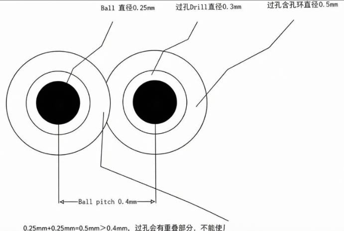
VFBGA chips feature extremely fine ball pitch (typically 0.4 mm). Conventional multilayer boards rely on mechanical drilling, which fundamentally conflicts with such fine pitches:
The minimum hole diameter achievable with standard mechanical drilling is 0.3 mm. Including the annular ring, the total via footprint diameter reaches approximately 0.5 mm—already larger than the 0.4 mm ball pitch. Attempting to route under these conditions inevitably causes overlap between adjacent pads and vias, leading to short circuits and making proper fan-out impossible.
This leads to a widely accepted industry rule: Only when the BGA ball pitch is ≥ 0.65 mm can mechanical vias with 0.3/0.5 mm specifications be used for routing, eliminating the need for HDI processes.
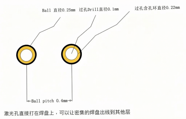
In contrast, HDI boards employ laser microvias with diameters as small as 0.1 mm. Including the annular ring, the total diameter is only about 0.22 mm, allowing direct placement on BGA pads as small as 0.25 mm. Within a 0.4 mm pitch, laser microvias avoid spatial interference or short-circuit risks, enabling perfect fan-out for fine-pitch VFBGA packages.
In summary, fan-out routing for fine-pitch VFBGA chips fundamentally depends on laser microvias—an exclusive HDI process—thus mandating the use of high-end HDI boards for such chips.
Prerequisite Core Process Knowledge
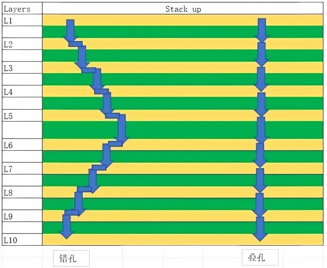
I. Stacked Via vs. Staggered Via (Two Stacking Methods for HDI Laser Microvias)
Stacked Via: Laser microvias in vertically adjacent layers are perfectly aligned concentrically, forming a continuous copper column that enables direct connections from outer to inner layers (e.g., L1→L3). This method requires the lower-layer microvia to be fully filled with copper and polished flat before the upper-layer microvia can be drilled and laminated. It involves two lamination cycles, two laser drilling steps, and two electroplating/filling processes.
Staggered Via: Laser microvias in adjacent layers are laterally offset, with interlayer connectivity achieved through short traces on intermediate layers. This approach does not require full copper filling of the lower-layer microvia—only via wall plating is needed—resulting in lower processing difficulty and cost.
ELIC (Every Layer Interconnect) boards can flexibly combine both stacked and staggered vias. In practice, stacked vias are preferred due to their space-saving nature and shorter signal paths, which significantly enhance signal integrity and power integrity.
II. Key Differences Among Blind Vias, Buried Vias, and Through Vias
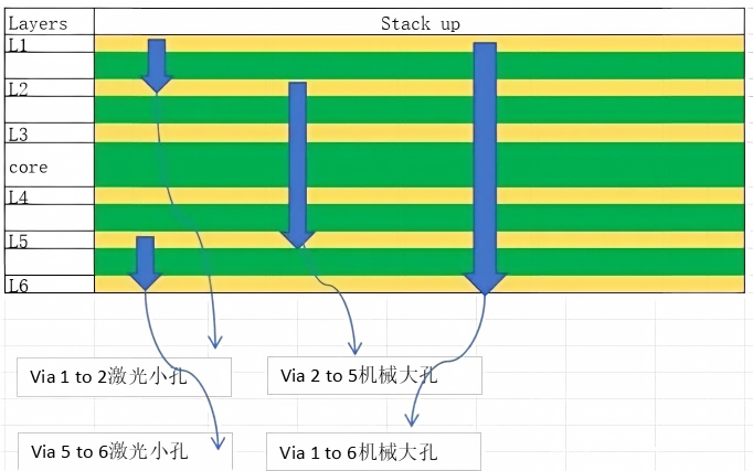
PCB vias are categorized into three types based on their penetration depth, using an 8-layer HDI-2 board as an example:
Blind Via: Connects only the outer layer to an adjacent inner layer, with one end exposed on the board surface and the other terminating within the dielectric, without penetrating the entire board. Examples in an 8-layer board include L1–L2 and L7–L8 vias.
Buried Via: Entirely embedded within the board, invisible from both top and bottom surfaces, connecting only internal layers without involving outer layers. Example: L3–L6 via in an 8-layer board.
Through Via: Mechanically drilled to penetrate all layers, serving as the primary interconnect method in conventional multilayer boards. Example: L1–L8 full-through via in an 8-layer board.
Detailed Process Characteristics of HDI Board Levels
1. HDI-1 (1st-build HDI, Standard Stackup: 1+N+1)
One sequential lamination and one laser microvia process are performed on each side of the core substrate (where N is the number of core layers). Internal layer interconnections are limited to mechanical through vias and buried vias, restricting design flexibility.
Key Features: Blind vias connect only adjacent layers (e.g., L1–L2 or outermost to second-outermost layer), do not support via stacking, and cannot achieve skip-layer connections (e.g., L1–L3). Typical stackup: 6-layer 1st-build HDI is 1+4+1.
2. HDI-2 (2nd-build HDI, Standard Stackup: 2+N+2)
Two sequential laminations and two rounds of laser drilling are performed on each side of the core substrate, making it the most widely used mid-to-high-end industrial process.
Key Features: Supports dual-layer blind vias (L1–L2 and L2–L3), compatible with both stacked and staggered configurations; enables direct routing from the outer layer to layer 3 without requiring through-via detours, significantly simplifying routing and reducing signal loss. Typical stackup: 8-layer 2nd-build HDI is 2+4+2.
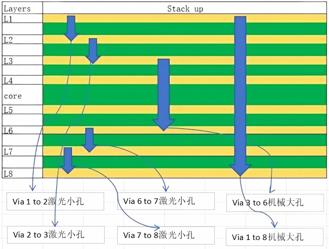
3. HDI-3 (3rd-build HDI, Standard Stackup: 3+N+3)
Three sequential laminations and three laser blind via processes are performed on each side of the core substrate. Common configurations include 8-layer (3+2+3) and 10-layer (3+4+3).
Key Features: Supports three consecutive stacked laser blind vias (L1–L2, L2–L3, L3–L4), enabling stepped blind vias and complex buried via structures; stacked vias allow direct outer-to-layer-4 connections, greatly enhancing multi-layer routing capability to meet high-density, high-speed chip requirements.
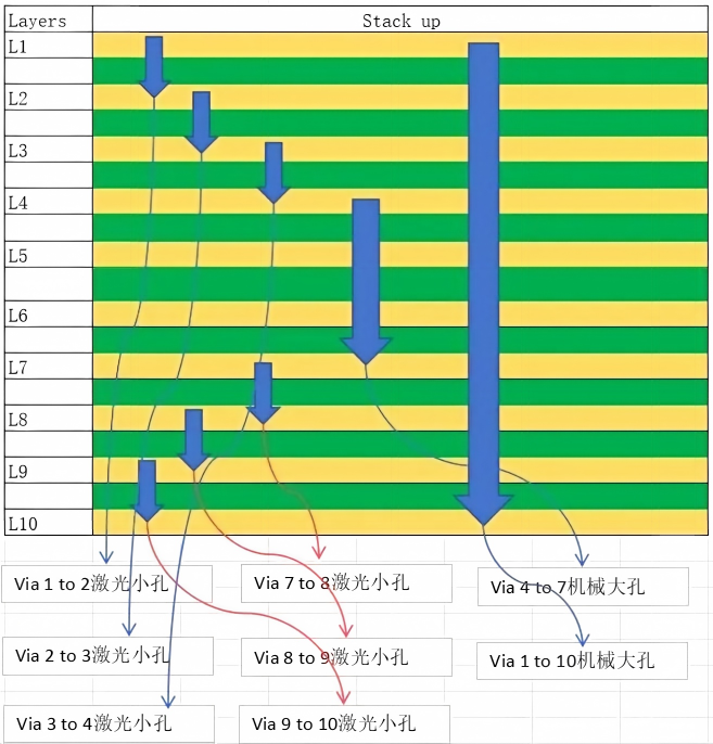
4. ELIC (Every Layer Interconnect Board, Top-Tier HDI Process)
Traditional HDI-1/2/3 boards retain a solid thick core substrate, within which only mechanical buried vias can be used—laser blind vias cannot span across the core, limiting routing flexibility. In contrast, ELIC employs a high-end thick-core-free structure (not "coreless," but built by alternately laminating multiple thin dielectric and copper foil layers).
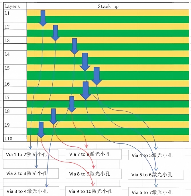
Key Features: Laser microvias can be formed between any two adjacent layers, unrestricted by the number of outer buildup layers. There is no fixed 3+N+3 stackup rule, enabling the shortest possible interlayer paths and maximum routing freedom—ideal for ultra-high-density precision designs.
Process Limitation: If the board thickness is large (e.g., 1.6 mm), the thick core cannot be eliminated. Since the core cannot be laser-drilled and only allows mechanical drilling, even with multiple buildup layers, such boards can at best achieve HDI-4—not ELIC. For example, a 10-layer board with a thick core is limited to HDI-4, not ELIC.
Answers to Extended Thinking Questions
Question 2: Are all PCBs with blind and buried vias classified as HDI boards?
Not necessarily. The defining criterion for HDI is not merely the presence of blind or buried vias, but rather the fabrication method of the blind vias. If blind vias are created using laser microvias, the board qualifies as HDI; if they are made by traditional mechanical drilling—even with blind/buried structures—it remains classified as a conventional multilayer PCB.
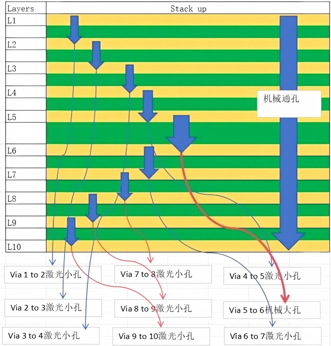
Question 3: How is a full L1–L10 through via implemented in a 10-layer ELIC board?
ELIC mass production relies primarily on stacked laser microvias. All multi-layer interconnections are achieved through cascaded laser blind vias, using exclusively laser drilling throughout. Although mechanical through vias are cheaper, manufacturers avoid introducing additional mechanical drilling steps in volume production to prevent process contamination that could compromise precision and reliability. (In rare special applications, a few mechanical through vias may appear at the board periphery as exceptions, but this does not affect the board’s classification as ELIC.)
trending news
Contact Us