



Sorry, no sales person is available right now to take your call. Pls leave a message and we will reply to you via email as soon as possible.
Home/ PCB News/ AMB Ceramic Substrates: A Comprehensive Overview of Processes, Technologies, Advantages, and Applications
AMB Ceramic Substrates: A Comprehensive Overview of Processes, Technologies, Advantages, and Applications
2026-08-28
Technical Principles and Manufacturing Process
AMB (Active Metal Brazing) is a specialized welding technology that enables high-strength bonding between ceramics and metals. Its core principle lies in using a brazing filler metal containing small amounts of active elements (such as Ti or Zr), which chemically reacts with the ceramic surface at high temperatures to form a reactive interfacial layer that can be fully wetted by the molten filler metal, thereby achieving a metallurgical bond between the ceramic substrate and oxygen-free copper layer.
The typical fabrication process for AMB ceramic substrates is as follows:
Filler Metal Coating: The active metal brazing alloy is uniformly applied onto the ceramic substrate surface via screen printing;
Assembly and Brazing: The coated ceramic substrate is stacked and clamped with an oxygen-free copper layer, then placed into a vacuum brazing furnace for high-temperature bonding;
Circuit Patterning: Photolithography and etching techniques are used to fabricate the desired circuit patterns on the copper surface;
Surface Finishing: The patterned circuits undergo chemical plating (e.g., nickel/gold plating) to enhance solderability and oxidation resistance.
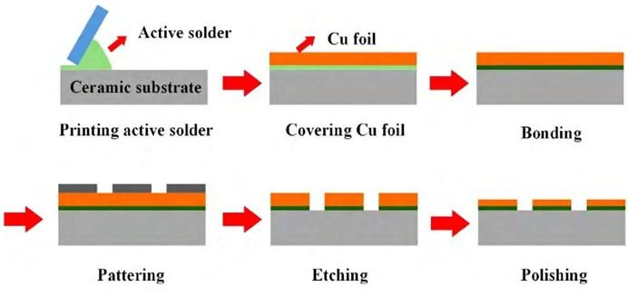
The general method for manufacturing AMB ceramic substrates is as follows: First, apply active metal brazing alloy onto the ceramic substrate surface via screen printing; then assemble it with an oxygen-free copper layer and perform high-temperature brazing in a vacuum furnace; next, etch the copper layer to form circuit patterns; finally, apply chemical plating to the patterned surface.
Comparison Between AMB and DBC Processes
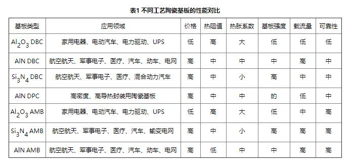
AMB technology can be regarded as an advanced evolution of the DBC (Direct Bond Copper) process. The key differences between the two are as follows:
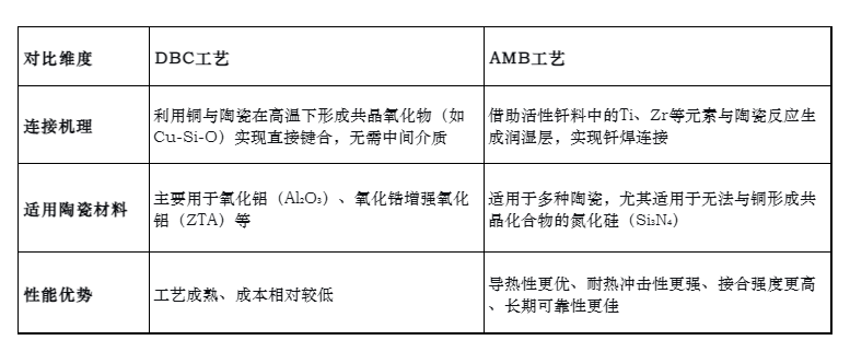
It should be specifically noted that silicon nitride (Si₃N₄) and copper cannot form an effective Cu-Si-O eutectic phase, making the DBC process inapplicable; thus, reliable bonding must rely on AMB technology.
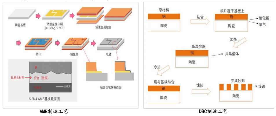
The DBC technique bonds copper directly to ceramics without additional materials, whereas AMB uses active metals to braze copper onto ceramics.
Compared to DBC, AMB offers superior thermal conductivity, higher thermal stability, greater mechanical strength, and enhanced reliability.
Silicon nitride Si3N4 does not form Cu-Si-O compounds with copper, so the DBC process cannot be used; the AMB process must be employed to achieve bonding between silicon nitride and copper.
Comparison of Cross-sectional Structures of DBC and AMB Substrates
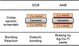
Reliability of AMB Ceramic Substrates
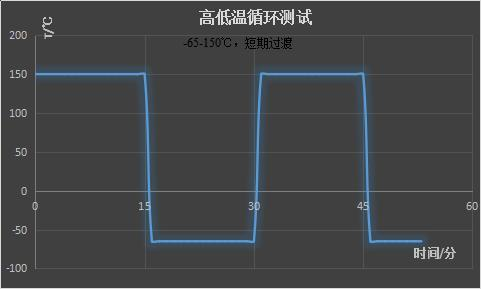
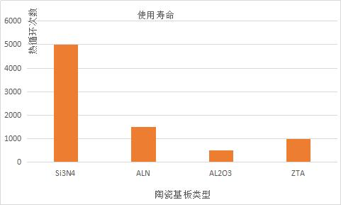
Thermal cycling testing is a critical metric for evaluating the reliability of ceramic覆copper substrates. A typical test condition is: temperature range from -65°C to +150°C (ΔT = 215°C), with 15 minutes dwell time at each extreme temperature and transition time not exceeding 2 minutes. The cycling lifetimes of different ceramic substrates are as follows:
Si3N4 ≥ 5000 cycles;
AlN ≥ 1500 cycles;
Al2O3 ≥ 500 cycles;
ZTA (zirconia-toughened alumina) ≥ 1000 cycles
It is evident that silicon nitride-based AMB substrates exhibit far superior durability under extreme thermal cycling conditions compared to other materials, which constitutes their core advantage in high-reliability applications.
Market Potential and Drivers
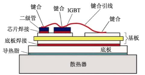
As power modules continue evolving toward higher voltage, higher current, and greater power density, merely enhancing chip performance is no longer sufficient to meet the dual demands of system miniaturization and high efficiency. Innovative packaging technologies—particularly substrate solutions offering excellent thermal management and high reliability—have become a critical breakthrough.
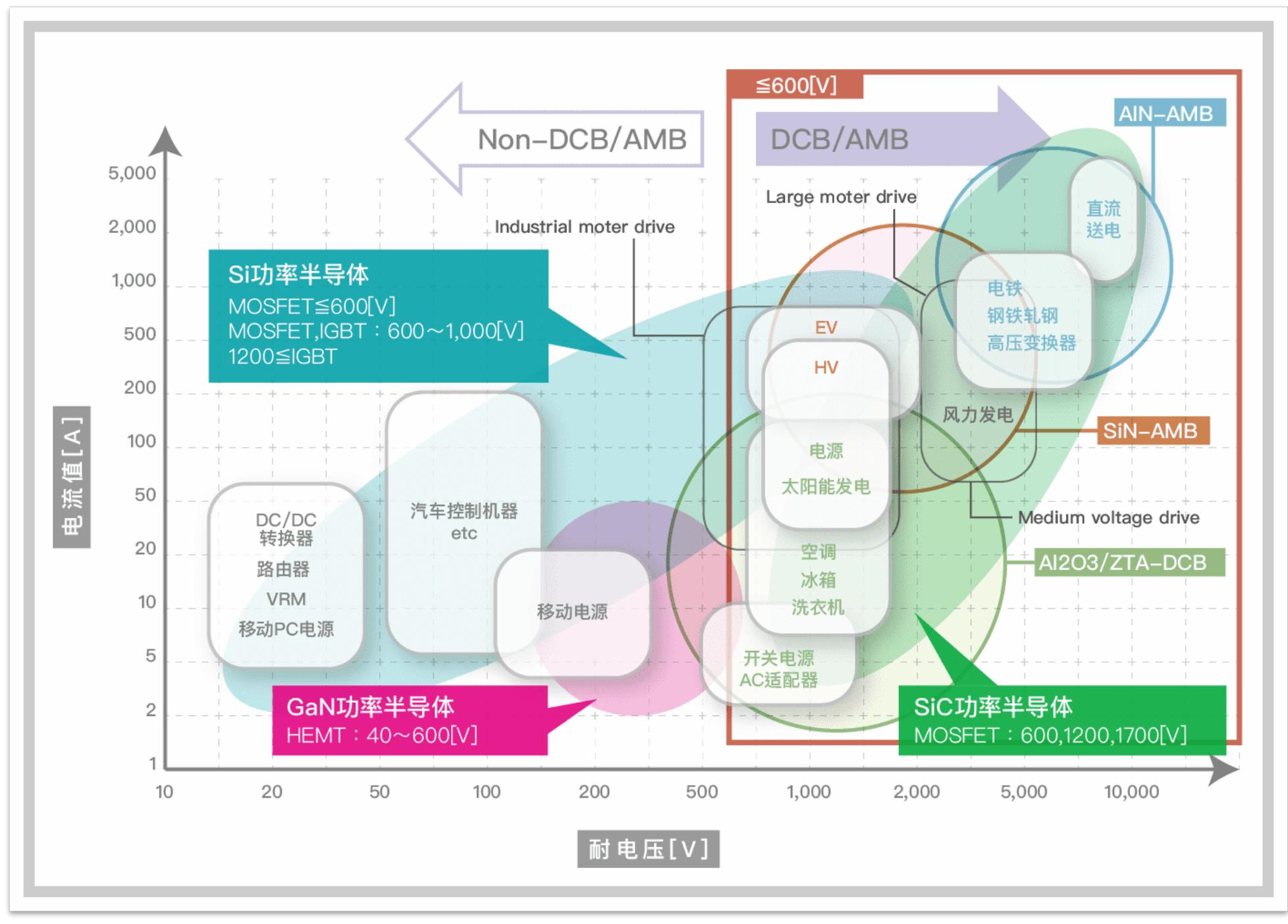
Thanks to its exceptional thermal conductivity, thermal stability, and mechanical strength, AMB ceramic substrates are gradually becoming the preferred substrate solution for high-performance power modules. Especially in the field of third-generation semiconductor (e.g., SiC) power devices, silicon nitride AMB substrates are widely recognized as the optimal choice due to their closely matched coefficient of thermal expansion (CTE) with SiC chips, which significantly reduces thermal stress and enhances long-term module stability.
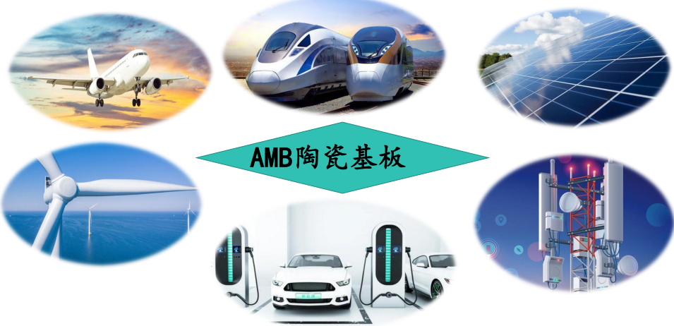
Furthermore, in traditional power modules based on silicon IGBTs, AMB substrates are rapidly replacing conventional DBC substrates in demanding applications such as rail transit, industrial drives, electric vehicles, and smart grids—where stringent requirements exist for thermal performance, reliability, and power rating—leading to continuously rising market penetration.
Industry Chain Structure
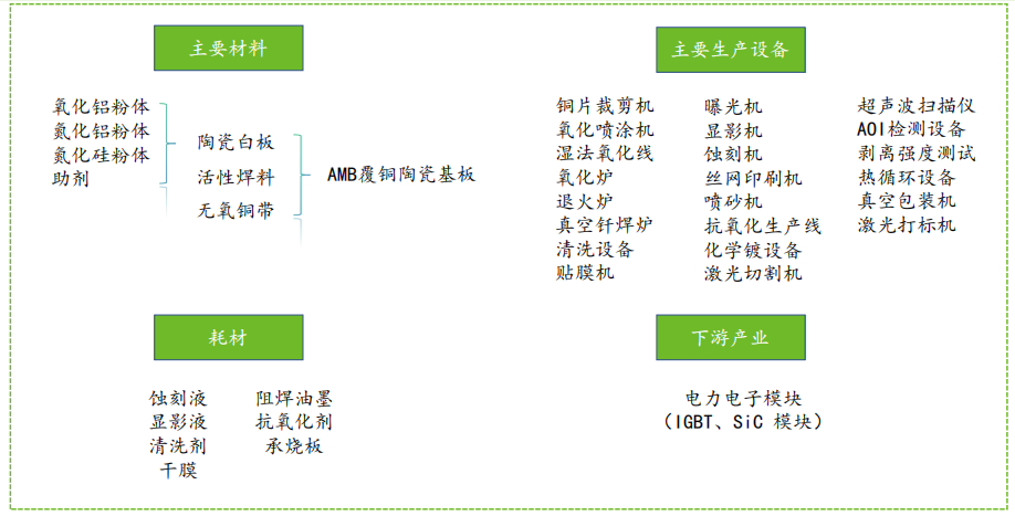
The AMB ceramic substrate industry chain encompasses upstream raw materials, midstream manufacturing consumables and equipment, and downstream application modules, as detailed below:
Main Raw Materials
Alumina powder, aluminum nitride powder, silicon nitride powder, various additives, green ceramic tapes, active metal brazing alloys, oxygen-free copper strips.
Key Consumables
Etchants, developers, cleaning agents, dry films, solder masks, anti-oxidants, setter plates, etc.
Main Production Equipment
Copper sheet cutting machines, oxidation spray coaters, wet oxidation lines, oxidation furnaces, annealing furnaces, vacuum brazing furnaces, cleaning equipment, laminators, exposure systems, developers, etchers, screen printers, sandblasters, anti-oxidation production lines, electroless plating equipment, laser cutters, ultrasonic scanners, AOI inspection systems, peel strength testers, thermal cycling test chambers, vacuum packaging machines, laser marking machines, etc.
Downstream Application Areas
Power electronic modules, primarily IGBT modules and SiC power modules, widely serving high-end equipment sectors such as rail transit, electric vehicles, photovoltaic inverters, smart grids, and industrial motor drives.
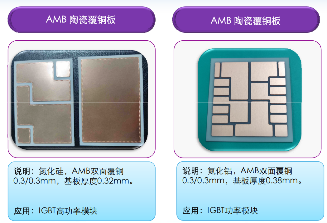
Baineng Yunban AMB Process Ceramic Substrates
Conclusion
With its unique material compatibility, outstanding thermal dissipation capability, and ultra-high reliability, AMB ceramic substrates have become an indispensable foundational packaging material for high-power, high-frequency, and high-temperature applications. As third-generation semiconductors achieve large-scale commercialization and the new energy industry experiences rapid growth, AMB technology will continue to drive innovation and market expansion in power module substrates.
trending news
Contact Us