



Sorry, no sales person is available right now to take your call. Pls leave a message and we will reply to you via email as soon as possible.
Home/ PCB News/ Baineng Cloud Board | Full Analysis of the 6-Layer RO4350B + IT180A High-Frequency Hybrid Lamination Process
Baineng Cloud Board | Full Analysis of the 6-Layer RO4350B + IT180A High-Frequency Hybrid Lamination Process
2026-08-25
What Challenges Does RF PCB Face in the 5G Massive MIMO Era?
As 5G base stations evolve from Sub-6GHz to millimeter wave, the number of RF channels has surged from 4T4R to 64T64R or even 128T128R. Under the Massive MIMO architecture, the Active Antenna Unit (AAU) integrates power amplifiers (PAs), low-noise amplifiers (LNAs), RF transceiver circuits, and antenna feed networks—all on a single board carrying both multi-gigahertz RF signals and numerous digital control signals.
This presents PCB substrate materials with an apparently contradictory requirement: RF channels demand extremely low dielectric loss and stable dielectric constant, while digital control layers require high Tg, high thermal resistance, and cost-effectiveness. An all-high-frequency board offers excellent performance but at prohibitively high cost, whereas an all-FR-4 solution suffers severe loss degradation above 3 GHz. Hybrid laminate technology emerged precisely to address this dilemma and has become the mainstream architecture for 5G RF PCBs.
Why Choose “Hybrid Lamination”?—The Engineering Optimum Between Performance and Cost
The core principle of hybrid lamination is material zoning: RF signal layers are placed on low-Dk, low-Df high-frequency substrates, while power, ground, and digital signal layers use high-Tg FR-4 material. Both materials are integrated through a single lamination process.
Taking a 6-layer hybrid board as an example, a typical stack-up strategy is as follows:
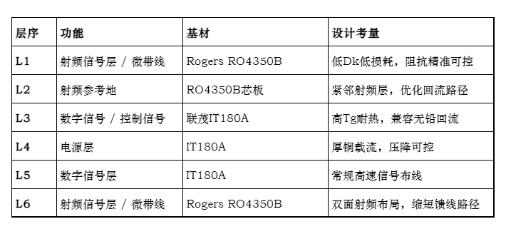
The immediate benefits of this architecture include: RF performance approaching that of an all-high-frequency board, 30%–50% reduction in material cost, and retention of the high reliability and standard process compatibility of FR-4 layers.
In-Depth Material Selection: The Synergy Between RO4350B and IT180A
RF Layer Substrate: Rogers RO4350B
RO4350B is a ceramic-filled hydrocarbon laminate developed by Rogers Corporation for commercial RF applications, with key electrical parameters as follows:
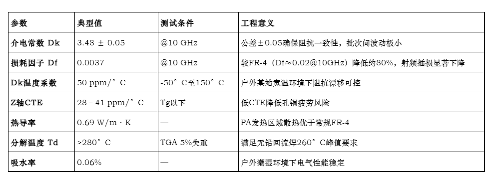
The key advantage of RO4350B lies in its process compatibility: unlike pure PTFE substrates that require plasma treatment and special bonding films, RO4350B can be processed using standard epoxy/glass fabric techniques—drilling, copper plating, and lamination can all be performed on conventional PCB production lines. This compatibility is a critical reason why RO4350B has become the de facto standard for 5G base station RF boards.
Digital/Power Layer Substrate: ITEQ IT180A
ITEQ IT180A is a high-Tg (175°C–180°C) multifunctional filled epoxy resin substrate designed as a high-reliability upgrade to standard FR-4:
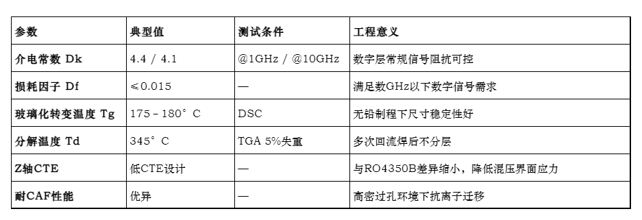
The rationale for selecting IT180A centers on balancing thermal resistance and CAF resistance: 5G AAU boards typically feature high-density designs with minimum via diameters of 0.4 mm and 4/4 mil trace/space. With dense vias and elevated operating temperatures, IT180A’s low CTE and high Td effectively suppress Conductive Anodic Filament (CAF) growth and via copper fracture risks.
Key Process Parameters and Engineering Implementation for 6-Layer Hybrid Boards
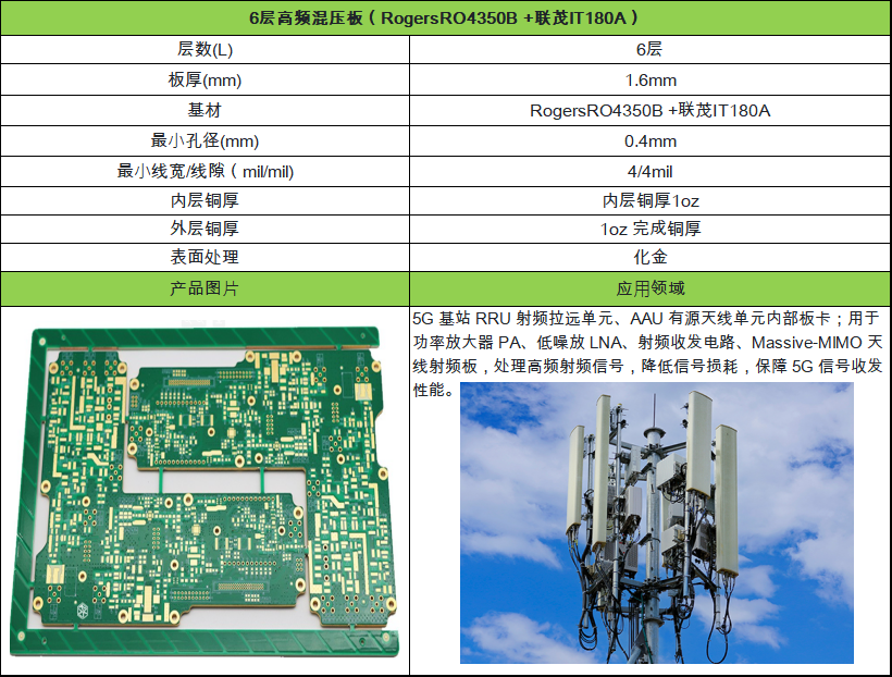
Taking a mass-produced 6-layer high-frequency hybrid board from BaiNeng CloudPCB as an example, key manufacturing parameters are as follows:
Impedance Control: Conventional Formulas Don’t Apply
Impedance calculation is the first engineering hurdle for hybrid boards. Since RO4350B (Dk=3.48) and IT180A (Dk=4.1 @10GHz) have different dielectric constants, and the effective dielectric thickness may slightly vary due to prepreg (PP) flow during lamination, directly applying conventional impedance models often results in measured values deviating from design targets by more than ±10%.
Standard engineering practice includes:
Using field solvers (e.g., Polar Si8000/9000) for stack-up modeling, inputting Dk and Df values for both materials separately;
Ensuring RF microstrip lines reference a solid ground plane of the same material, avoiding cross-material referencing;
Conducting first-article impedance testing before lamination and fine-tuning trace width compensation based on measured results;
Sampling impedance coupons per batch during mass production, maintaining tolerance within ±10% (±7% for critical RF traces).
Lamination Process: CTE Mismatch Is the Root Cause of Delamination
The core challenge in hybrid lamination lies in the difference in Z-axis CTE between the two substrates. RO4350B has a Z-axis CTE of approximately 28–41 ppm/°C, while standard FR-4 ranges from 50–70 ppm/°C. During lamination heating to 180°C and subsequent reflow peak temperatures of 260°C, interfacial shear stress can exceed 12 MPa, potentially causing delamination or uneven PP flow if not properly controlled.
BaiNeng CloudPCB employs the following integrated approach in mass production:
① Symmetrical Stack-Up Design
The 6-layer board adopts a symmetrical structure: “high-frequency – FR4 – FR4 – high-frequency,” with L1/L6 made of RO4350B and L3/L4/L5 of IT180A, separated by matched prepreg (PP) layers to balance thermal expansion forces and limit warpage to under 0.75%.
② Segmented Lamination Profile Control
Ramp rate: 2–3°C/min (slower than the standard FR-4 rate of 4–5°C/min) to reduce internal stress from asynchronous heating;
Soak stage: Hold at 120°C–140°C for 20–30 minutes to allow full PP flow and outgassing;
Cure stage: Hold at 180°C–185°C for 60–90 minutes to ensure complete curing of the IT180A system;
Cooling stage: Controlled at 2–3°C/min to prevent thermal shock-induced interfacial stress concentration.
These parameters are based on BaiNeng CloudPCB’s actual process window for 6-layer hybrid boards and should be fine-tuned according to press model and PP batch.
③ Interfacial Bonding Material Selection
Low-flow prepreg (PP) or Rogers-specific bonding films (e.g., 4450F) are recommended between RO4350B and FR-4 to strictly control resin flow and prevent excessive resin squeeze-out in the high-frequency layer, which could shift Dk values.
Drilling and Via Metallization: Managing Drilling Smear at Bimaterial Interfaces
Drilling hybrid boards faces the challenge of differing machinability between the two materials: RO4350B’s softer resin tends to leave adherent drilling smear on via walls, while IT180A’s hard fillers accelerate drill wear. At 0.4 mm hole diameters, incomplete smear removal can lead to poor copper adhesion or voids in via walls.
Standard process flow:
Drill bit selection: Use UC (Under Cut) bits with 130°–140° point angles to minimize entry burrs;
Feed rate: Slightly reduce feed speed (10–15 μm/rev) for RO4350B layers and increase slightly for IT180A layers;
Smear removal: Combine plasma cleaning + chemical micro-etching for RO4350B sides, and standard potassium permanganate desmear for IT180A sides;
Via copper thickness: Electroless + electrolytic copper plating, average thickness ≥25 μm, meeting IPC Class 3 requirements.
By combining segmented feed rates and plasma cleaning, BaiNeng CloudPCB achieves consistent via copper adhesion exceeding IPC Class 3 standards in 0.4 mm hybrid board mass production, with batch yield exceeding 98%.
Dimensional Stability Control: Managing the “Personality” of High-Frequency Materials
RO4350B exhibits different X/Y-axis dimensional stability compared to FR-4. Without proper compensation after multilayer lamination, misalignment between inner-layer patterns and drilled holes can occur. Engineers must measure the actual dimensional change of each core before lamination and apply differential compensation in drilling programs to maintain layer-to-layer alignment within ±0.075 mm.
Typical 5G RF Application Scenarios
This 6-layer RO4350B + IT180A hybrid board is specifically targeted at 5G base station RF front-end applications. BaiNeng CloudPCB’s product has been mass-deployed in RRU and AAU products from multiple telecom equipment manufacturers, covering PA/LNA boards and Massive MIMO feed networks in Sub-6GHz bands.
Internal Boards in RRU (Remote Radio Unit) / AAU (Active Antenna Unit)
RRUs and AAUs are the RF cores of 5G base stations, requiring simultaneous handling of RF signals and digital control signals. The hybrid architecture places PA output matching networks and LNA input matching networks on RO4350B layers, while ADC/DAC interfaces, power management, and control buses reside on IT180A layers—achieving an optimal balance between RF performance and system integration.
PA Power Amplifiers and LNA Low-Noise Amplifiers
PA output signals can reach several to tens of watts, making them sensitive to dielectric loss and thermal conductivity. LNA inputs demand ultra-low noise figures, where dielectric loss directly impacts overall system noise performance. RO4350B’s Df = 0.0037 @10GHz ensures low insertion loss in RF paths, while its thermal conductivity of 0.69 W/m·K effectively aids heat dissipation in PA regions.
Massive MIMO Antenna RF Feed Boards
In 64T64R+ arrays, the antenna feed network includes numerous microstrips, power dividers, and couplers. Trace/space precision directly affects array amplitude/phase consistency. The combination of 4/4 mil fine-line capability and RO4350B’s stable Dk ensures phase coherence and cross-polar discrimination (XPD) across large-scale arrays.
Selection Recommendations and Engineering Tips
For hardware teams evaluating 5G RF board solutions, the following recommendations are worth noting:
Not all high-frequency layers require RO4350B: Signal layers operating below 3 GHz can consider high-speed FR-4 materials like IT180A for further cost optimization;
Ensure solid RF reference planes: Avoid split grounds beneath RF microstrips, as this causes impedance discontinuities and increased radiation;
ENIG surface finish outperforms OSP: For RF contact points subject to repeated mating or soldering, ENIG offers superior contact resistance stability compared to organic solderability preservatives;
Never skip first-article validation: Impedance, warpage, and via reliability of hybrid boards must be thoroughly verified during prototyping. Prior to mass production, it’s recommended to complete temperature cycling tests (-40°C to +85°C, ≥100 cycles);
Choose a manufacturer with hybrid lamination experience: Hybrid board yield heavily depends on the production line’s accumulated expertise in lamination profiles, drilling parameters, and impedance compensation. Prioritize PCB vendors with proven 5G RF board mass production records.
In the high-frequency hybrid board domain, BaiNeng CloudPCB has established end-to-end capabilities—from material selection and stack-up design to lamination process—and has achieved stable mass production of 6-layer RO4350B + IT180A hybrid boards for multiple telecom equipment manufacturers’ 5G RF projects. For R&D teams with hybrid lamination needs, we recommend involving the manufacturer early in the design phase for stack-up review to proactively mitigate risks related to impedance deviation, warpage, and delamination from a manufacturability perspective.
Conclusion
The complexity of 5G RF front-ends continues to escalate—evolving from Sub-6GHz to millimeter wave and expanding from 64T64R to even larger arrays—placing increasingly stringent demands on PCB materials and processes. As a mature, mass-production-proven architecture, high-frequency hybrid lamination will remain the mainstream choice for 5G RF boards for the foreseeable future. A deep understanding of RO4350B and IT180A material characteristics and precise control over key hybrid process parameters are essential competencies for every RF hardware and PCB process engineer. BaiNeng CloudPCB remains committed to advancing high-frequency hybrid technology, delivering reliable and efficient PCB solutions for 5G and next-generation communication equipment.
trending news
Contact Us