





















Sorry, no sales person is available right now to take your call. Pls leave a message and we will reply to you via email as soon as possible.
Company Profile
Click to view more about BainengAbout Baineng
BNI ELECTRONICS (THAILAND) CO.,LTD. is a subsidiary of the Baineng-Kinji Group. Founded in 1997, the Group's parent company, Shenzhen Baineng Information Technology Co., Ltd., stands as a national innovation benchmark in the electronic components and PCB industry. It holds the prestigious dual recognition of being both a National High-Tech Enterprise and a specialized and sophisticated "Little Giant" enterprise. Through its deeply integrated online and offline (OMO) platform, the company has built an intelligent supply chain system centered on a "PCB and components dual-engine" model, providing global customers with one-stop services ranging from product design and R&D to supporting manufacturing.Headquartered in Shenzhen, the Group has branch offices in South China, East China, Hong Kong, Taiwan, Thailand, and other regions, employing over 400 staff members. It operates 6 major business divisions, 2 online trading platforms, and 2 research institutes. With products and services reaching 28 countries and regions worldwide, the Group has served more than 2 million customers and counts leading renowned companies across industries such as new energy, automotive, security, lighting, medical, home appliances, and industrial control among its downstream clients.
Global Distribution
Founded in 1997, we are a national high-tech enterprise in the electronic components industry. Headquartered in Shenzhen, we have established branch offices in South China, East China, Hong Kong, Taiwan, and other regions, with a current workforce of over 400 employees. Our operations are organized into six major business divisions and two research institutes. Our products and services have reached 28 countries and regions worldwide, serving 2 million users.
Five Core Competencies
-
Brand Influence
Brand Influence -
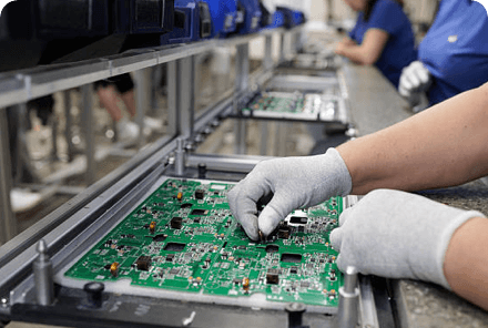
Supply Chain Capacity
Supply Chain Capacity -

Customer Service Capability
Customer Service Capability -
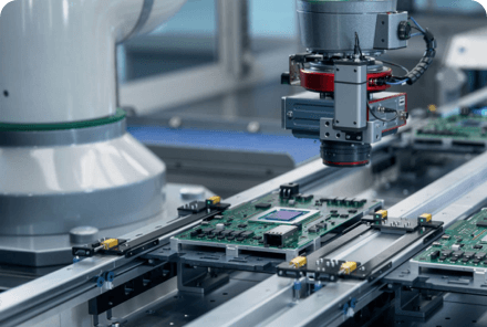
Software and Hardware Technology Development Capabilities
Software and Hardware Technology Development Capabilities -

The Ability to Cultivate Professional Talents
The Ability to Cultivate Professional Talents
Development History
2020
2021
2022
2025
News and Updates More Articles >
2026/10/15

<div class="article-content"> <p>光模块PCB设计“分段金手指”主要基于以下几个关键原因:</p> <ul> <li><strong>信号完整性优化</strong>:高速差分信号(如10G/25G/40G/100G)对阻抗连续性要求极高。分段设计允许在不同区域独立控制阻抗匹配,减少反射和串扰。</li> <li><strong>电源与地隔离</strong>:将电源引脚、地引脚和信号引脚物理分离,可有效降低噪声耦合,提高信噪比(SNR),确保模拟前端(AFE)和数字逻辑的纯净供电。</li> <li><strong>机械可靠性与插拔寿命</strong>:分段结构可缓解整体应力集中,避免单一长条金手指在频繁插拔中因弯曲或磨损导致接触不良,提升连接器耐久性。</li> <li><strong>功能分区明确</strong>:便于按功能划分引脚组(如TX/RX数据对、I²C管理接口、电源VCC/GND、热插拔检测等),简化布线布局,降低交叉干扰风险。</li> <li><strong>兼容性与标准化</strong>:遵循MSA(多源协议)标准(如SFP+、QSFP28等),确保不同厂商模块间互操作性,同时支持未来速率升级时的引脚复用需求。</li> </ul> <p>简言之,“分段金手指”是高速光通信领域平衡电气性能、机械可靠性和标准化要求的工程最优解。</p> </div>
<p>Optical modules are high-speed communication devices that perform optical-electrical/electrical-optical conversion. Typical products consist of optical components, electrical chips, PCBs, structural parts, and heat dissipation components. The PCB is inserted into one end of equipment such as switches and servers, typically featuring gold-plated contact areas, commonly known as "gold fingers." So-called "segmented gold fingers" are not merely an aesthetic design choice; rather, they involve arranging and isolating the contact areas according to different electrical functions.</p>
Read more2026/10/14
Analysis of Main Manufacturing Processes for Ceramic Thick and Thin Film Substrates
<p>A typical multilayer co-fired ceramic thick-thin film circuit substrate is usually composed of two parts: the center is an HTCC multilayer ceramic body, and the top and bottom surfaces feature thin-film metallization with fine wiring. Its manufacturing process generally consists of two stages: first, a multilayer ceramic substrate is fabricated using the HTCC process; then, fine circuits are created on the front and back surfaces of the substrate using thin-film technology.</p>
Read more2026/10/13
High-Density Integrated Packaging Thermal Dissipation Breakthrough: Vertical Heat Dissipation Pathway of Chip-Copper Block-Copper Column-AMB Ceramic Substrate
This paper proposes a high-density integrated packaging vertical heat dissipation scheme based on "chip—copper block—solid copper-plated pillar—AMB ceramic copper-clad substrate". This scheme embeds copper blocks with pre-soldered chips within multilayer boards, and forms a low-thermal-resistance, predominantly metal/ceramic vertical thermal conduction path through solid copper-plated pillars and the bottom AMB ceramic substrate, providing a feasible engineering path for improving heat dissipation and reliability of high-power density devices.
Read more2026/10/08
Embed First, Metallize Later: An Analysis of Low-Cost Embedded Ceramic PCB Technology
To enhance the insulation and heat dissipation performance of PCBs, ceramics can be embedded into the PCB substrate. Ceramics have a low coefficient of thermal expansion (CTE), and their embedding also helps improve the dimensional stability of PCBs, meeting the requirements of high-precision surface mount components. This differs from the process of directly embedding metallized Active Metal Brazing (AMB) ceramic substrates
Read more2026/10/14

<title>Power Bank New National Standard Compliance: YXC Yangxing Technology RTC Achieves Cost-Effectiveness and Rapid Compliance</title>
<p>The "Safety Technical Specification for Power Banks" (GB 47372—2026) is scheduled to be officially released in April 2027. Electronic design's real-time clock (RTC) chip—the YSN8563 series—can help manufacturers meet the new national standard requirements with low cost and minimal modifications.</p>
Read more2026/10/08
XINGLIGHT Digital Tube: Solving the Challenges of Scattered Selection, Chaotic Driving, and Difficult Production Line Adaptation
<p>Chengxing Optoelectronics has launched a new series of digital tube products, building a comprehensive display device product matrix around multi-dimensional requirements including segment-based multi-color display, dot-matrix stepped size layout, compatibility with both common-cathode and common-anode dual-drive architectures, plug-in multi-digit combinations, and surface-mount automation line adaptation.</p>
Read more2026/09/11
YSO150HT Wide-Temperature Active Crystal Oscillator | Preferred Clock Solution for Integrated Joint Modules of Humanoid Robots
YSO150HT is a wide-temperature active crystal oscillator launched by YXC Technology, capable of supporting stable output across the full temperature range of -40°C to +125°C. It is perfectly suited for the high-temperature environments generated by humanoid robot joint modules during high-speed operation.
Read more2026/03/19

Congratulations! BAINENG Achieves Dual Authoritative Certifications Again – All Four Management Systems Fully Compliant, Accelerating High-Quality Development
Recently, Shenzhen BaiNeng Information Technology Co., Ltd. has announced another significant achievement in its management system development! Following its successful certification under the ISO9001 Quality Management System and the Intellectual Property Management System, the company has now also successfully obtained certifications for the ISO14001 Environmental Management System and the ISO45001 Occupational Health and Safety Management System.
Read more2026/01/17
ONE KINJI, ONE GOAL - A Warm Gathering, Thankful for the Journey Together - The Spring Festival Customer Appreciation and Awards Banquet Kicks Off Warmly.
In the warm winter at year's end, our bonds grow deeper; under the twinkling lights, we embark on a new chapter together. On January 17, 2026, following the successful conclusion of the group's annual target operation summary meeting, the "ONE KINJI · ONE GOAL" New Year Customer Appreciation and Awards Dinner commenced warmly. Partners, industry friends, and members of the Kinji family from all corners gathered together, setting aside a year of busyness to reminisce about the times of shared struggle amid laughter and joy. In the glow of shared glory, we set out on the journey toward mutual success in 2026.
Read more2026/01/17
Unite in Heart, Move Forward Together, Gather Momentum, Embrace the New — Group's 2025 Annual Goal Management Summary Meeting Successfully Held
Following the BPO debriefing meeting on January 16, 2026, the Group's 2025 Annual Target Management Summary Meeting was grandly held at Shenzhen Tairan Licheng on January 17. Senior executives of the Group, heads of various business units (GPO/BPO), and key members of the middle and back offices gathered to build on the outcomes of the previous day's business review. The meeting focused on the annual summary and planning of middle and back office departments, with the core objectives of aligning perspectives, pooling efforts, and ushering in a new phase. Participants reviewed the Group's overall performance in 2025 and laid out the strategic blueprint for 2026.
Read more2026/01/16
Gathering Momentum for Future Endeavors, Advancing with Determination — The Group’s 2025 BPO Accountability Report Meeting Concludes Successfully
On January 16, 2026, the Group’s BPO Review Meeting for 2025 was successfully convened. Centered on the theme of "Review for Improvement and Communication to Build Consensus," the meeting comprehensively reviewed the strategic execution outcomes of each Business Unit (BP) over the past year, discussed development plans for 2026, and promoted the in-depth implementation of the Group’s AI digital transformation and financial compliance enhancement strategies. Key personnel from across the Group gathered to discuss growth and embark on a new journey together.
Read more2022/12/05
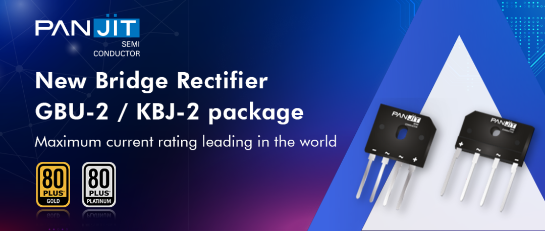
ON Semiconductor Launches New Generation GBU-2 / KBJ-2 Bridge Rectifiers
Qiangmao has launched a new generation of GBU-2/KBJ-2 bridge rectifiers, with rated currents ranging from 4A to a maximum of 35A. The new bridge rectifiers optimize the internal structure, enhance heat dissipation performance, and achieve optimal thermal conductivity. The design significantly reduces power loss, making them particularly suitable for high-current and high-wattage power supply systems.
Read more2022/12/01
Qiangmao Launches New Product DXK Bridge Rectifier
Cyntec has launched a new generation of 2-8A, 1000V DXK packaged, general series bridge rectifiers, featuring improved forward surge current and high-temperature, low reverse leakage current characteristics. Intelligent manufacturing optimizes production parameters to provide bridge products with lower power consumption, thereby enhancing system efficiency.
Read more2022/09/16
Industry's Most Complete 200V Automotive-Grade Ultra-Fast Recovery Rectifier Diodes.
PANJIT has launched automotive-grade 200V ultra-fast recovery rectifiers, the MER&MSR series products, with rated currents ranging from 1A to 20A. Thin packages include SOD-123FL, SOD-123HE, SMA, SMB, SMAF-C, and SMBF, suitable for replacing conventional axial-lead or MELF components in surface-mount applications. High-power packages include TO-220AC, ITO-220AC, TO-220AB, and ITO-220AB, with a total of 62 products launched, 25 of which are AEC-Q101 certified.
Read more2022/09/07
Low Voltage Low Noise HTC863XA/HTC72XA Rail-to-Rail Series Operational Amplifiers Introduction
The HTC863XA and HTC72XA are low-noise, low-voltage, and low-power operational amplifiers. These series of chips can be used in a very wide range of applications. Their input common-mode voltage range extends to ground, with maximum input offset voltages of 4.2 mV and 3.5 mV, respectively. Under heavy loads, they can provide rail-to-rail output swings. The HTC863XA operates with a single supply voltage ranging from +2.3V to +5.5V, while the HTC72XA operates with a single supply voltage ranging from +2.5V to +5.5V. The operating temperature for the chips ranges from -40°C to +125°C.
Read more