



Sorry, no sales person is available right now to take your call. Pls leave a message and we will reply to you via email as soon as possible.
Home/ PCB News/ Explanation of HDI Stack-up, Impedance Process, and Structural Optimization for Eight-layer Boards
Explanation of HDI Stack-up, Impedance Process, and Structural Optimization for Eight-layer Boards
2026-06-29
This article systematically elaborates the mainstream stack-up architectures, lamination process characteristics, and core mass production challenges of 8-layer 1-step, 2-step, 3-step, and anylayer HDI printed circuit boards. Combining advanced PCB industry design practices and mass production experience, it proposes systematic structural optimization strategies tailored to different HDI step counts, aiming to simplify manufacturing processes, lower production barriers, reduce manufacturing costs, and simultaneously enhance board structural stability and mass production yield—providing standardized technical references for engineering design and scalable manufacturing of high-frequency, high-speed, and high-density HDI products.
1. 8-Layer 1-Step HDI Board (Single Build-Up, Two Laminations)
The 8-layer 1-step HDI board is the most widely used single build-up type in consumer electronics and industrial control applications. Its industry-standard symmetric stack-up is 1+6+1, following the general 1+N+1 design paradigm (where N ≥ 2 and N is even). This board type employs a two-lamination process, with buried vias pre-formed in the inner core layers, resulting in a final product integrating surface blind vias and inner buried vias. The overall process is mature, highly stable, and offers a wide tolerance margin for mass production, making it the standardized preferred solution for basic 8-layer HDI mass production scenarios.
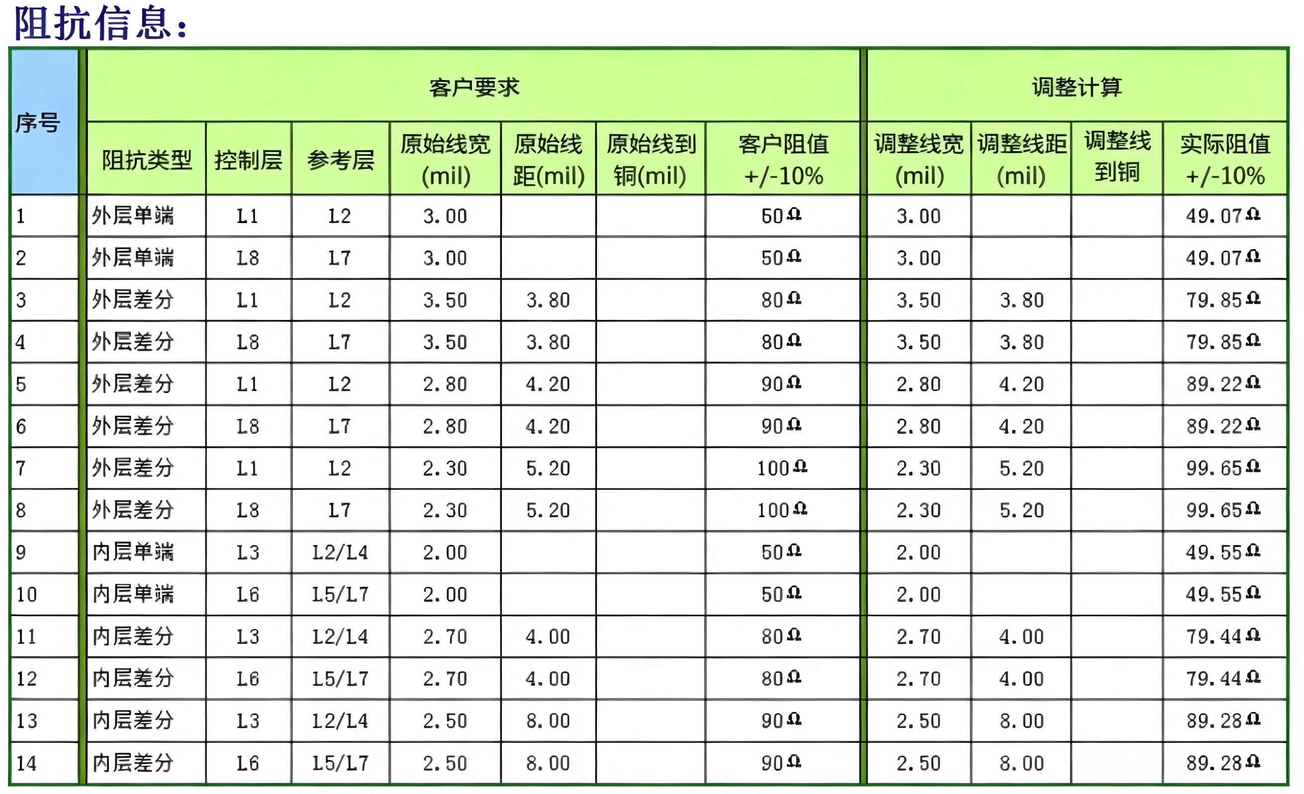
Key Impedance Design Considerations
The symmetric and balanced 1+6+1 stack-up offers excellent dielectric uniformity and structural symmetry, resulting in outstanding overall impedance consistency. It meets standard impedance control requirements such as 50Ω single-ended traces and 90Ω/100Ω differential pairs within the board. The outer signal layers L1 and L8 use the adjacent sub-surface copper layers as complete reference planes, enabling strong control over dielectric thickness. Under mass production conditions, impedance tolerance can be stably maintained within ±5%, satisfying typical electrical performance specifications for high-frequency circuits.
The inner 6-layer core allows flexible allocation of power, ground, and signal layers. Design must strictly adhere to the fundamental principle that signal layers must be adjacent to ground layers. Signal layers must never be sandwiched between two power layers to avoid impedance drift and signal crosstalk caused by missing reference planes. Additionally, consistent via diameter compensation and solder mask opening optimization should be applied to all blind and buried vias to ensure uniform copper exposure around vias, preventing localized copper thickness variations or dielectric stress imbalances that could cause impedance deviations and ensuring consistent trace impedance across the entire board.
2. Conventional 8-Layer 2-Step HDI Board (Double Build-Up, No Stacked/Skip Vias)
The conventional 8-layer 2-step HDI board without skip vias features an industry-standard symmetric stack-up of 1+1+4+1+1, following the general structure 1+1+N+1+1 (where N ≥ 2 and N is even). This is the mainstream standardized architecture for double-build HDI. Buried vias are pre-formed in the inner layers, requiring three lamination cycles for full fabrication. With no stacked vias or skip-layer blind vias, this structure presents moderate process complexity and is compatible with stable mass production by most PCB manufacturers.
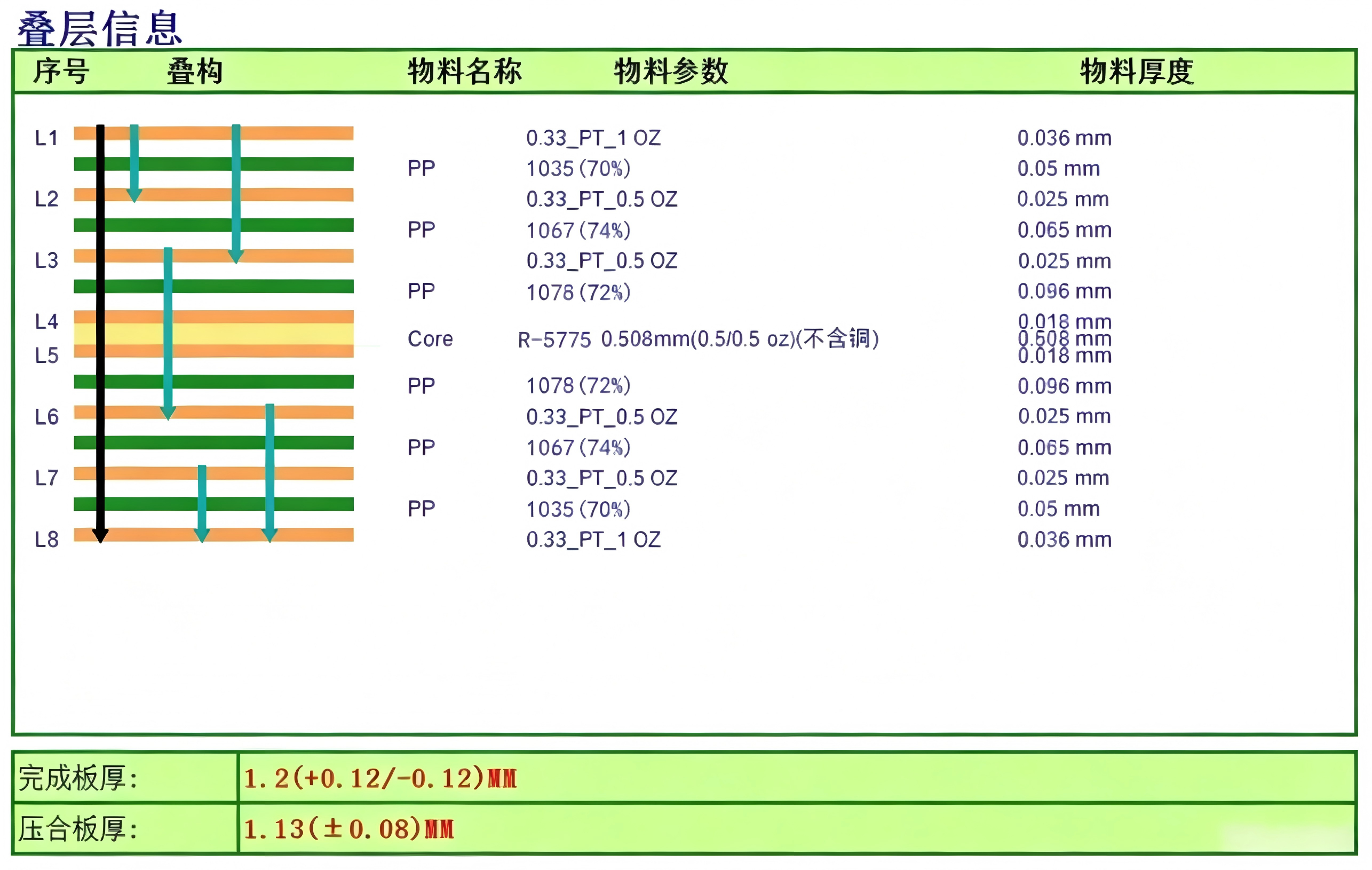
This structure offers significant room for process optimization: The traditional buried via layout between layers 3–6 can be optimized to layers 2–7. Without altering electrical performance, mechanical strength, or interconnect logic, this change eliminates one lamination step, effectively simplifying the production flow and reducing combined material and process costs—making it the core optimization strategy for low-cost, high-yield 2-step HDI mass production.
Key Impedance Design Considerations
The symmetric 1+1+4+1+1 build-up structure features thin build-up dielectrics, high interlayer consistency, and excellent symmetry—making it ideal for high-precision impedance design. It meets stringent ±3% impedance control standards required by high-frequency, high-speed products. Signal traces on outer layers L1/L8 and sub-outer layers L2/L7 each have dedicated, adjacent ground reference planes, resulting in excellent linearity for both single-ended and differential impedance. The clear relationship among trace width, dielectric thickness, and impedance value facilitates batch production control and parameter calibration.
The optimized 2–7 buried via structure completely avoids the cross-dielectric-layer defects inherent in traditional 3–6 layouts, effectively reducing risks of impedance anomalies caused by via-area dielectric delamination or thickness variation. During design, build-up dielectric thickness tolerances must be tightly controlled, and routing should be zoned according to signal speed. High-speed differential pairs must avoid dense via regions to prevent impedance discontinuities caused by clusters of blind and buried vias, thereby ensuring overall board impedance accuracy and consistency.
3. Skip-Blind-Via 8-Layer 2-Step HDI Board (Double Build-Up, High-Difficulty Variant)
The skip-blind-via 8-layer 2-step HDI board adopts the standard 1+1+4+1+1 stack-up but represents a high-difficulty variant of double-build 2-step HDI. Buried vias are placed between inner layers 3–6, requiring three lamination cycles. Its core process challenge lies in the stacked skip-blind-via design, which demands extremely high equipment precision, process control capability, and technical expertise—only manufacturers with advanced HDI mass production qualifications can achieve stable yields.
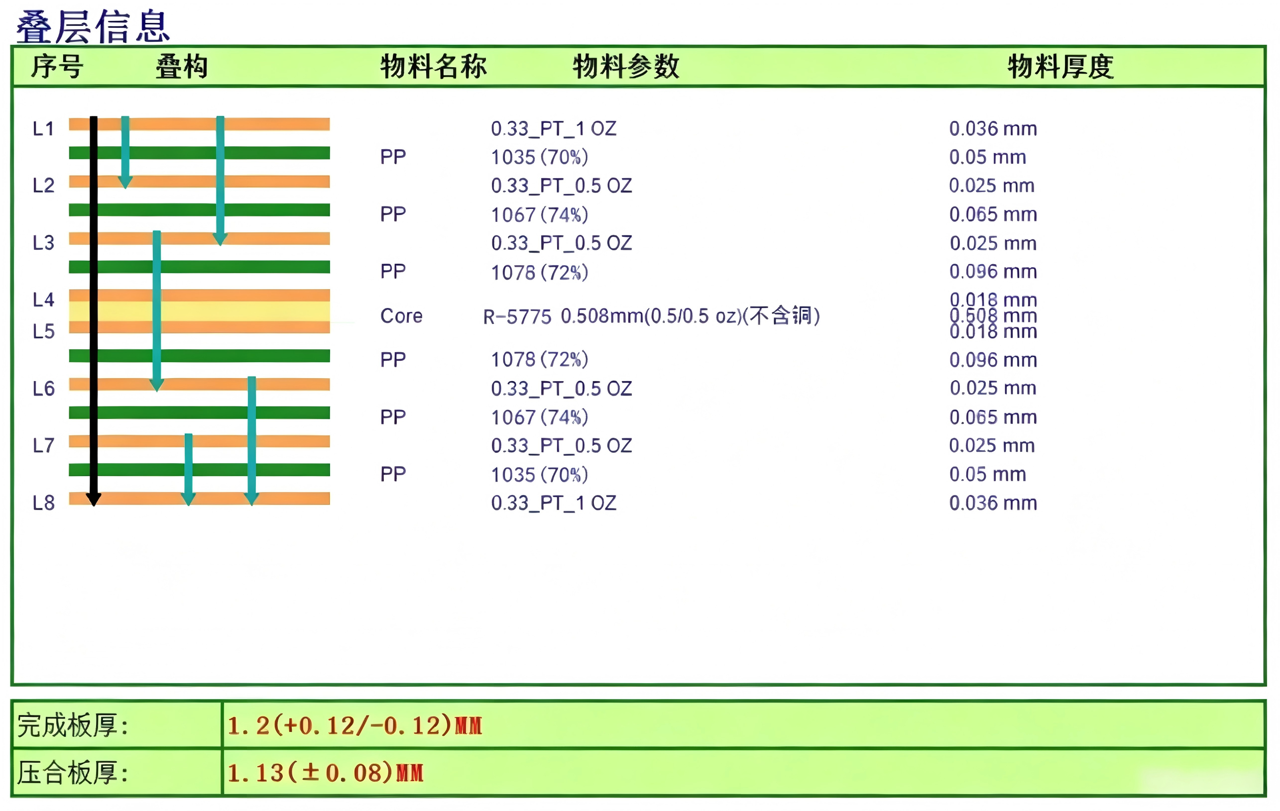
The primary bottleneck in manufacturing this structure centers on stacked skip-via formation: The 1–3 layer skip-blind via cannot be formed in a single laser step and must be split into two sequential processes: 1–2 and 2–3. The 2–3 inner blind via requires precision via-filling before the second lamination. Compared to standard non-filled 2-step HDI boards, this filling process significantly increases process complexity, scrap risk, and manufacturing cost.
To address these mass production challenges, the industry-standard optimization is: eliminate the traditional monolithic 1–3 stacked skip-blind via and replace it with offset 1–2 blind vias combined with 2–3 buried/blind vias. This approach fully satisfies interconnect and electrical performance requirements while avoiding the high-difficulty stacked skip-via process through structural offsetting—effectively reducing production difficulty and cost while improving yield. Therefore, stacked and skip-blind vias should be avoided whenever possible in standard 2-step HDI designs.
Key Impedance Design Considerations
Stacked vias and skip-blind vias are the primary impedance control challenges in this board type. Stacked via regions suffer from dielectric discontinuities and inconsistent copper thickness, easily causing impedance jumps, signal reflections, and degraded signal integrity. In the 1–3 segmented drilling + 2–3 via-filling process, surface flatness deviations in filled areas directly impact the impedance accuracy of nearby precision traces, greatly increasing electrical stability control difficulty.
In engineering design, mandatory clearance must be enforced around stacked and filled vias: high-speed impedance traces must maintain a minimum safe distance of 0.2mm from via edges, and precision impedance traces must never route across stacked via zones. After adopting the offset via optimization, the board’s dielectric continuity and reference plane integrity are effectively restored, eliminating impedance fluctuations caused by skip-layer vias. For this high-difficulty structure, it is recommended during mass production to relax the impedance tolerance for precision traces to ±5%, while applying standard controls for ordinary low-speed traces—balancing manufacturability with electrical performance stability.
4. Optimization of 8-Layer 3-Step and Anylayer HDI Board Structures
8-layer 3-step and anylayer HDI boards (requiring more than three laminations) can adopt the same stack-up simplification and process reduction strategies used for 1-step and 2-step HDI to achieve cost reduction, quality improvement, and efficiency gains. Traditional 8-layer 3-step HDI requires four lamination cycles, but targeted stack-up optimization can eliminate one lamination step—achieving full compliance with structural, electrical, and reliability requirements in just three laminations. This optimized approach has been validated in high-volume production. Many initial high-step HDI designs contain redundant lamination steps; after stack-up simplification, they achieve significantly improved yield, shorter lead times, and lower total manufacturing costs without performance degradation—making it a core technique for optimizing high-step HDI cost-performance ratios.
Key Impedance Design Considerations
8-layer 3-step and anylayer HDI boards feature multiple build-up layers and rich dielectric hierarchies, enabling multi-level precision impedance routing capable of meeting ultra-high-precision ±2%~±3% impedance control demands in high-frequency, high-speed, high-density applications. Their main impedance risks stem from structural discontinuities introduced by multi-step blind vias and anylayer interconnects. Multiple build-up layers can cause local dielectric thickness deviations and copper thickness non-uniformity, leading to trace impedance shifts.
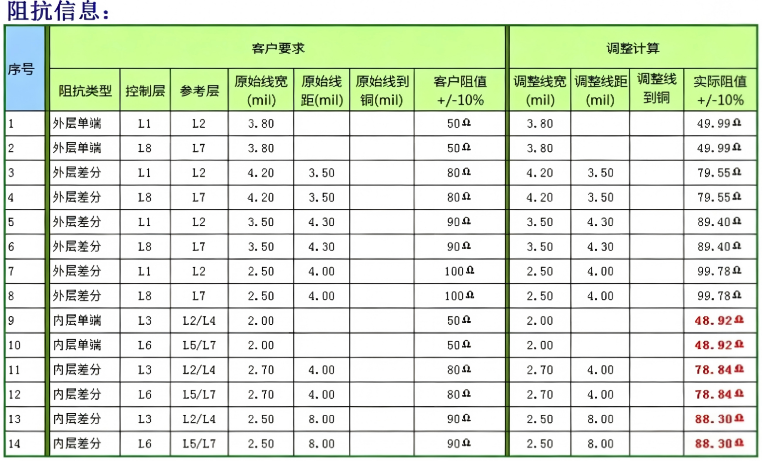
After lamination and stack-up optimization, board stack regularity improves significantly, and interlayer dielectric consistency is greatly enhanced—effectively reducing the difficulty of ultra-high-precision impedance control. Engineering design must strictly follow the principles of symmetric stacking and layer matching, standardizing dielectric thickness and copper foil specifications across all layers to ensure balanced and stable interlayer structure. High-speed impedance traces must be paired with dedicated reference ground planes, and routing across reference plane boundaries must be strictly prohibited. Additionally, specialized impedance compensation must be applied to all blind vias and anylayer interconnects—fine-tuning trace widths based on via diameter and spacing to offset impedance shifts caused by via structures, thereby ensuring stable, compliant impedance across all board layers.
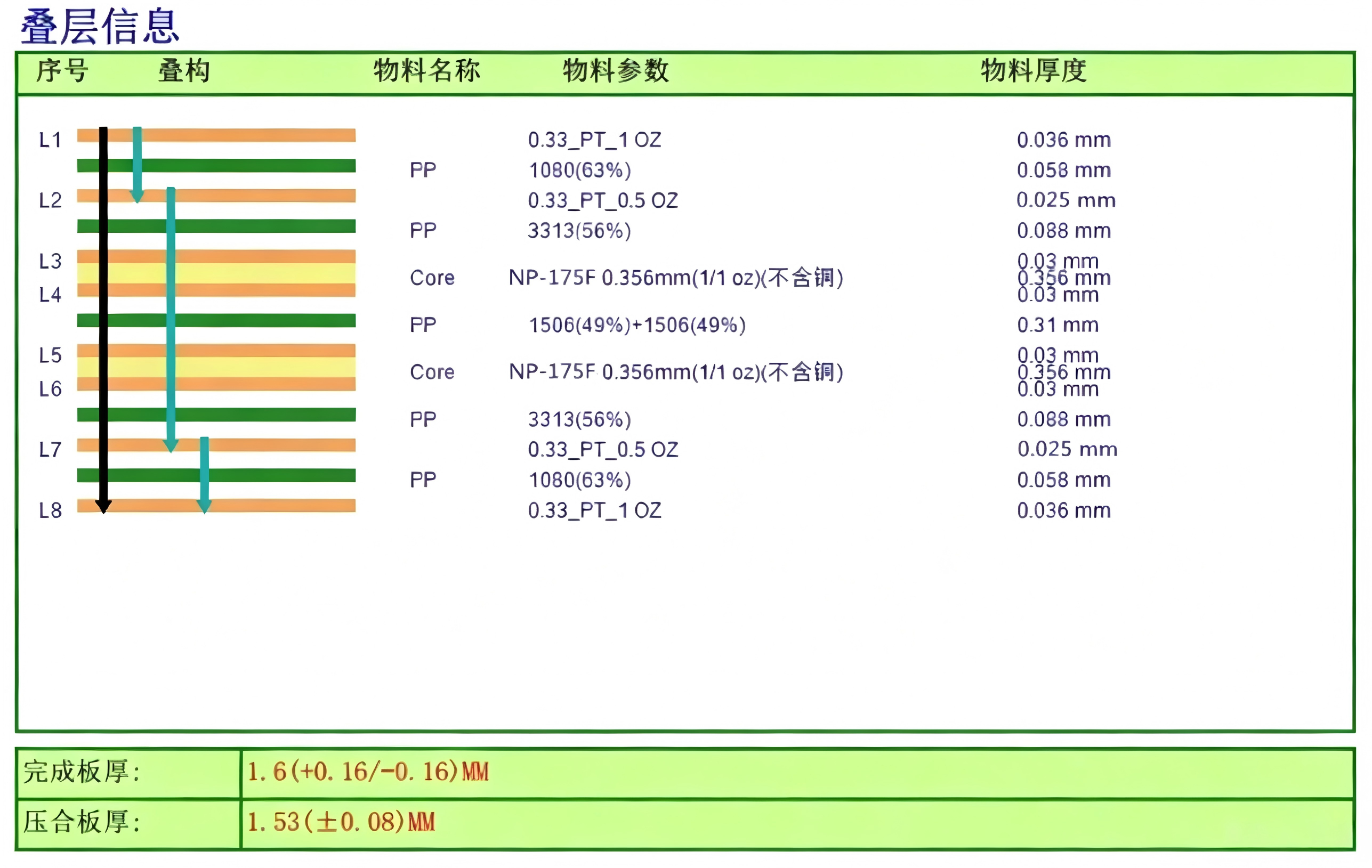
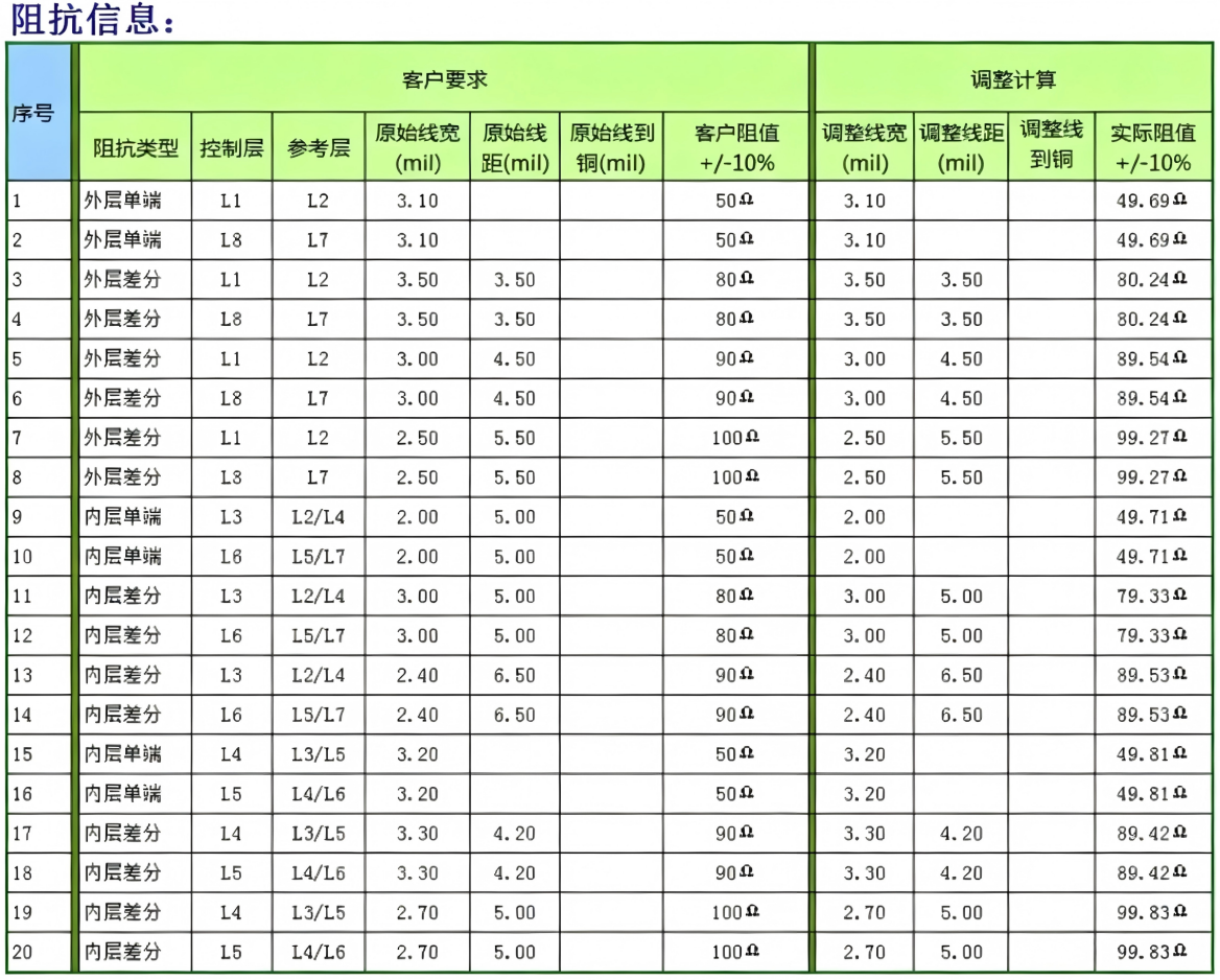
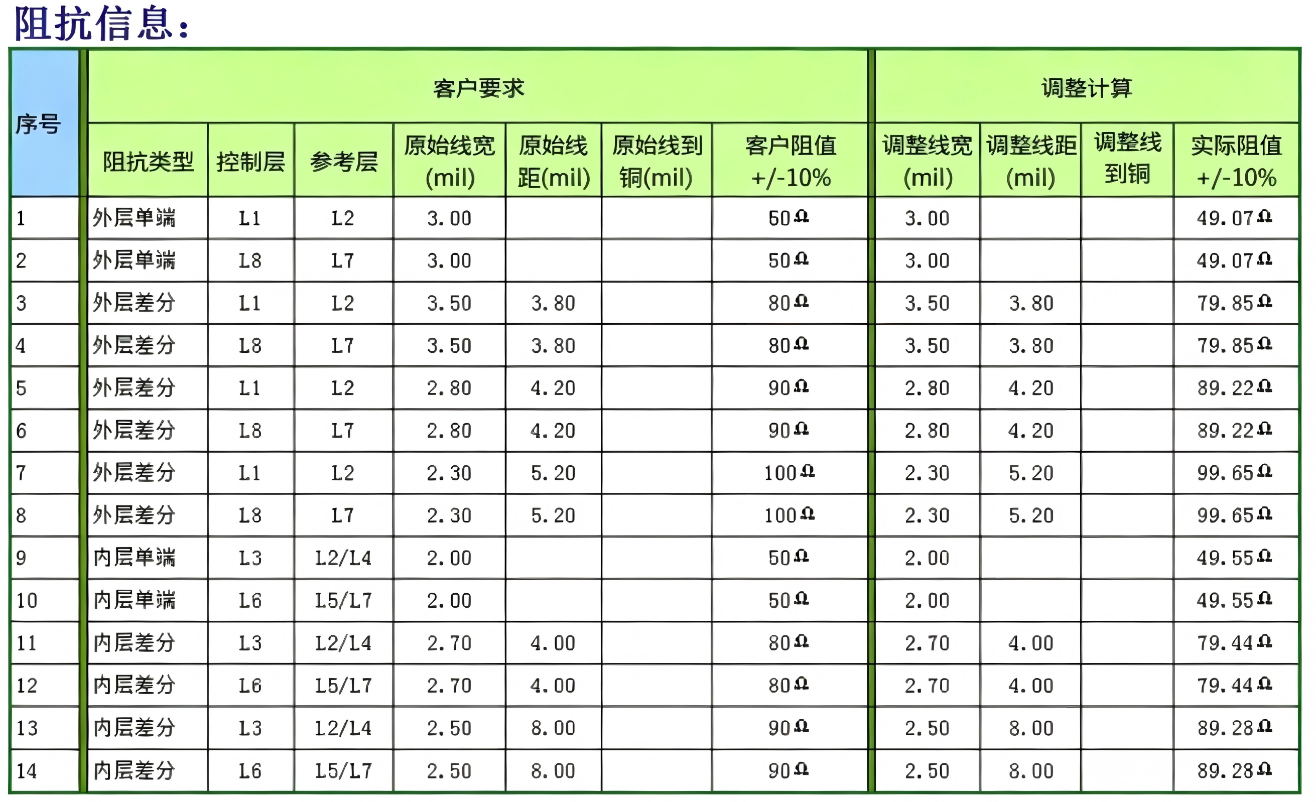
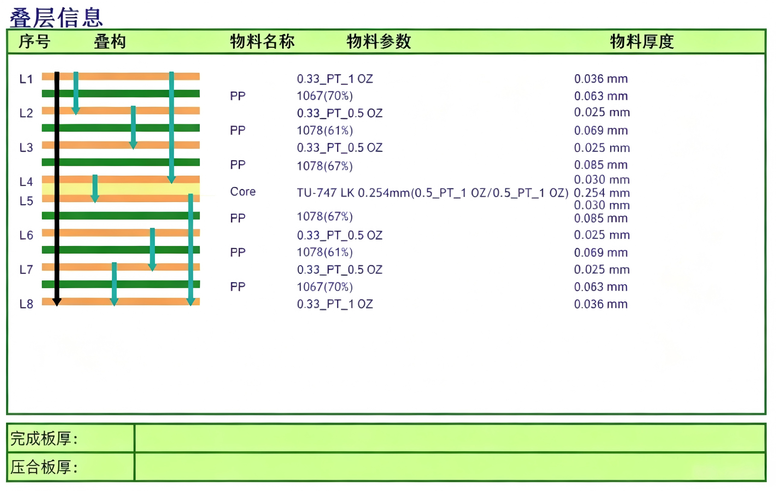
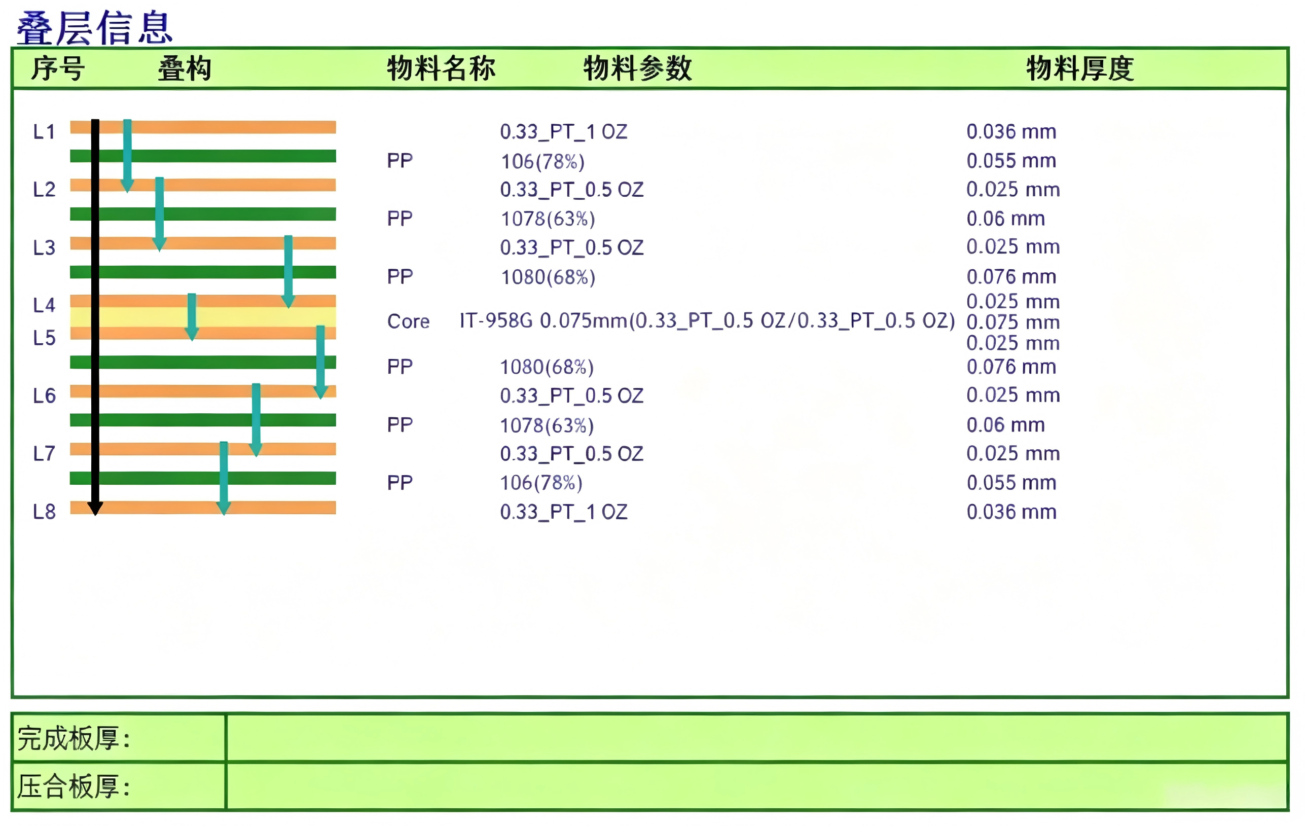
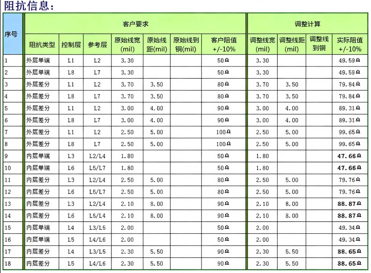
Below are the stack-up diagram and impedance information for an 8-layer anylayer HDI board.
trending news
Contact Us