



Sorry, no sales person is available right now to take your call. Pls leave a message and we will reply to you via email as soon as possible.
Home/ PCB News/ Building Uniform Fields Together, Thick Copper for High Power Handling | BAINENG Cloud Board 7oz Extra-Large Round High-End Specialty Thick Copper PCB
Building Uniform Fields Together, Thick Copper for High Power Handling | BAINENG Cloud Board 7oz Extra-Large Round High-End Specialty Thick Copper PCB
2026-06-26
In core areas of high-end equipment such as semiconductor vacuum processing, optical coating, precision heat treatment, and RF/millimeter-wave testing, the uniformity of the thermal field across the entire area, consistency of electromagnetic fields, and long-term operational stability directly determine process yield and equipment accuracy. These factors also represent critical technological barriers that have long constrained the advancement of China's high-end manufacturing. As equipment scales toward ultra-large dimensions, structural limitations of traditional rectangular PCBs are dramatically amplified—issues like board warpage, thermal field dispersion, electromagnetic non-uniformity, and insufficient current-carrying capacity can no longer meet the increasingly stringent requirements of cutting-edge applications.
With 26 years of deep expertise in high-precision specialty PCB manufacturing, Baineng Yunban directly addresses these core pain points in high-end manufacturing by independently developing ultra-large circular concentric specialty PCBs. Leveraging a proprietary concentric ring topology architecture combined with mature, mass-production-grade thick copper processes and vacuum-grade ultra-clean surface treatment technologies, the company fundamentally overcomes the industry-wide challenge of thermal and magnetic field non-uniformity on large-area boards. This delivers integrated, high-precision, highly stable, and highly adaptable carrier board solutions tailored for four key high-end sectors: semiconductors, photovoltaics & displays, precision heat treatment, and RF testing.
Core Advantages: Concentric Topology Architecture Redefines Uniformity Standards for Large-Area Thermal and Electromagnetic Fields
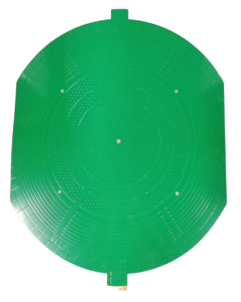
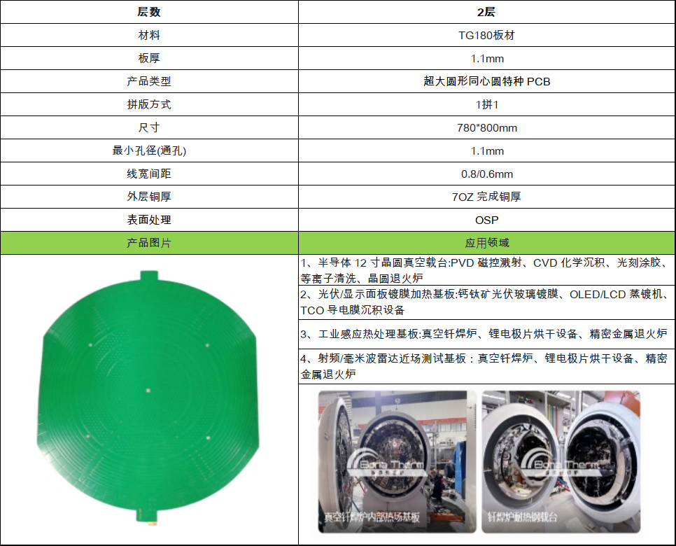
The product features a symmetrical dual-layer precision architecture that breaks through dimensional constraints, achieving a maximum finished diameter of 800mm with a standard board thickness of 1.1mm. It utilizes military-grade TG180 high-heat-resistant FR-4 substrate material capable of enduring continuous operation at 220°C, making it perfectly suited for high-vacuum, high-temperature, and high-intensity continuous industrial environments.
An innovative independent concentric ring circuit zoning technology modularizes the entire heating and radiation zones, enabling precise independent power control for each ring zone. This achieves micron-level uniform control over thermal, electromagnetic, and radiation fields, redefining industry standards for uniformity in large-area carrier boards.
Equipped with precision conductive gold fingers, a central reference positioning hole, and four corner high-accuracy mounting holes, the board ensures both high stability and durability in electrical connections while meeting micron-level alignment and integrated assembly requirements—striking a perfect balance between extreme precision and equipment compatibility.
7oz Thick Copper Board Product Showcase
Deep Empowerment Across High-End Applications, Precisely Matching Demands of Precision Manufacturing
Semiconductor 12-inch Wafer Vacuum Chuck
Compatible Equipment: Core process tools including PVD magnetron sputtering, CVD chemical vapor deposition, photolithography coating, plasma cleaning, and wafer annealing furnaces.
Core Value: Leveraging exclusive concentric zoned temperature control technology, the board achieves a surface-wide temperature variation of ≤±1°C, ensuring uniformity in wafer coating, deposition, and annealing processes from the source—significantly enhancing semiconductor process yield. Its proprietary vacuum-grade ultra-clean OSP process eliminates metal leaching and impurity release, preventing chamber contamination. It supports continuous operation at 160°C and short-term peak temperatures up to 200°C, fully meeting the extreme demands of advanced semiconductor processes.
Photovoltaic / Display Panel Coating Heating Substrate
Compatible Equipment: Optical coating systems for perovskite PV glass, OLED/LCD vacuum evaporation, and TCO conductive film deposition.
Core Value: Ultra-large surface area enables uniformly distributed heating, completely resolving issues like uneven optical film thickness and light transmission deviations in large-area coatings—significantly improving coating quality for PV glass and display panels. The 7oz thick copper layer supports extremely high currents, offering rapid thermal response and exceptional temperature stability, effectively reducing defects such as coating flaws, delamination, and color shifts, and driving optical processes toward higher quality and stability.
Industrial Precision Induction Heat Treatment Substrate
Compatible Equipment: Vacuum brazing furnaces, lithium battery electrode drying systems, precision metal annealing furnaces, and other high-end heat treatment equipment.
Core Value: Precision concentric ring coils generate a highly uniform electromagnetic induction field across the entire area, ensuring synchronous and balanced heating of workpieces. This overcomes traditional heat treatment issues such as excessive local temperature gradients, deformation, cracking, and performance inconsistency—guaranteeing high batch-to-batch uniformity and perfectly meeting the demands of high-precision metal processing.
RF / Millimeter-Wave Radar Near-Field Test Substrate
Compatible Equipment: 5G/6G RF modules, automotive millimeter-wave radars, phased array radars, and high-end near-field test fixtures.
Core Value: The precisely structured concentric ring circuitry creates a highly uniform and consistent electromagnetic radiation field, providing a stable, traceable, and repeatable test benchmark for 5G/6G RF modules, automotive radars, and phased array systems. This effectively avoids test errors caused by radiation non-uniformity in conventional carrier boards, significantly enhancing RF measurement accuracy and equipment calibration reliability.
Extreme Process Control: Building High-End Quality Barriers Through Stringent Standards
Baineng Yunban operates two advanced manufacturing bases in Shenzhen and Jiangxi, featuring 16,000㎡ of standardized cleanrooms and a monthly production capacity of 100,000㎡. Supported by a 200-member senior R&D team and 26 years of specialized PCB expertise, the company implements closed-loop control across 36 meticulous process steps. It holds multiple international certifications including UL, ISO9001, ISO13485, and IATF16949 (formerly TS16949), delivering highly stable and reliable core carrier boards for high-end equipment through industrial-grade stringent standards.
1. Precision Control of Large-Panel Deformation, Industry-Leading Flatness
To address stress-induced deformation in large panels, all base materials undergo 48 hours of pre-conditioning under constant temperature to relieve internal stress. Batch-specific thermal expansion coefficient compensation is applied to eliminate dimensional deviations at the source. Only Grade-A, high-stability, high-heat-resistant raw materials are used to establish a solid quality foundation. During lamination, segmented intelligent temperature control limits the heating rate to ≤2°C/min, combined with symmetrical stack-up precision techniques to completely eliminate unidirectional stress. Finished boards undergo full inspection on granite precision platforms, achieving warpage of ≤0.3%—perfectly matching the ultra-precise assembly and sealing requirements of high-end equipment.
2. Micron-Level Circuit Formation, Ultimate Concentric Precision
Large-format collimated light exposure technology ensures ring circuit line width uniformity within ±0.05mm, guaranteeing consistent specifications across all ring zones. The etching process employs an intelligent zoned spray pressure control system to precisely avoid common defects such as over-etching on outer rings or residual copper on inner rings. Interlayer alignment deviation is ≤0.04mm, complemented by full-area AOI automated optical inspection to detect even the smallest circuit imperfections. Positioning and reference holes are integrally formed with high precision, achieving overall concentricity of ≤0.03mm—ensuring perfect coaxial alignment of all ring zones for ultimate thermal and magnetic field uniformity.
3. Vacuum-Grade Ultra-Clean Processes for Extreme Cleanliness Environments
High-temperature-resistant matte green solder mask is precisely controlled to a thickness of 20–35μm—completely free of pinholes or bubbles—and releases no gases or impurities under high-temperature vacuum conditions, making it ideal for ultra-clean semiconductor and optical coating processes. The OSP anti-oxidation film thickness is maintained at 0.2–0.5μm, with multi-stage purification using 18MΩ ultrapure water to ensure zero ionic residue and zero metal leaching—preventing contamination of sensitive components and vacuum chambers. Gold-plated contact surfaces are ≥0.05μm thick, offering excellent wear resistance and oxidation protection for frequent plugging/unplugging cycles, ensuring long-term equipment reliability.
4. Comprehensive Electrical Performance Testing for Long-Term Reliability
Adhering to high-end quality control standards of 100% individual board inspection and full traceability: every board undergoes 100% circuit continuity testing to eliminate hidden faults like micro-breaks or latent opens; interlayer insulation withstands 2kV AC for 5 minutes with no breakdown or flashover, ensuring exceptional dielectric stability. Full-load temperature rise is precisely controlled—≤1°C surface variation for semiconductor-specific models and ≤3°C for general-purpose versions. After 100 thermal shock cycles between -40°C and 180°C, boards show no delamination, cracking, or performance degradation, demonstrating robustness in complex and extreme operating conditions.
5. Cleanroom Manufacturing + Vacuum Packaging Ensures Premium Delivery Quality
Critical processes—including etching, solder masking, OSP treatment, and precision cleaning—are conducted entirely in Class 10,000 cleanrooms to prevent particulate contamination at the source. Finished products are individually vacuum-sealed in anti-static packaging with dedicated protective structures and desiccant systems, eliminating risks of shipping damage, oxidation, or moisture absorption—delivering a premium "ready-to-use" experience.
Core Competitive Barriers: Setting the Benchmark for Domestic High-End Substitution
Stable Mass Production Capability for Ultra-Large Sizes: One of the very few domestic manufacturers capable of stable mass production of Φ800mm ultra-large circular PCBs, Baineng Yunban offers a complete chain from R&D prototyping and small-batch validation to scalable mass production—ensuring mature delivery and controllable lead times, thereby solving the industry-wide dilemma of “difficult to manufacture, difficult to scale, difficult to deliver” for ultra-large specialty PCBs.
Mature and Stable Thick Copper Process System: Standardized and mass-produced 7oz (245μm) ultra-thick copper technology has completely overcome core challenges of conventional thin-copper PCBs—such as high-temperature burnout, insufficient current capacity, and thermal runaway—ensuring long-term stability under high-power, high-temperature continuous operation. This process maturity leads the industry.
Vacuum-Specific Custom Solutions: A proprietary vacuum-grade OSP ultra-clean preparation process replaces traditional ENIG or HASL finishes prone to outgassing, achieving zero metal leaching and zero impurity release—exclusively tailored for the ultra-clean vacuum environments of semiconductor and optical coating equipment, delivering customized solutions for precision manufacturing.
Industry-Leading Precision Metrics: With three benchmark specifications—concentricity ≤0.03mm, circuit uniformity ±0.05mm, and warpage ≤0.3%—the company significantly exceeds general industry standards, establishing an ultra-precise physical foundation for high-end equipment requiring uniform thermal/electromagnetic fields and high-accuracy operation.
End-to-End Integrated Service: Offers a full range of specialty substrates and customized precision process solutions, covering concept iteration, structural optimization, sample validation, reliability testing, and volume delivery. Serving over 100,000 high-end manufacturing customers across 128 countries and regions, the company possesses extensive global experience in supporting high-end projects.
Empowering China’s High-End Manufacturing Advancement Through Precision Engineering
Today, high-end equipment is rapidly evolving toward ultra-large dimensions, ultra-high precision, extreme temperature/pressure conditions, and ultra-clean environments. PCBs have long transcended their role as basic circuit carriers—they are now core functional components that define the upper limits of equipment performance, production yield, and operational stability, and represent a pivotal element in the localization and advancement of high-end manufacturing.
With 26 years of industry dedication, Baineng Yunban leverages its groundbreaking concentric ring architecture, mature thick-copper precision processes, and rigorously controlled vacuum-clean technologies to deliver benchmark-level domestic alternatives characterized by high thermal uniformity, high field consistency, and high reliability. By continuously focusing on high-end sectors including semiconductors, photovoltaics, precision heat treatment, and RF testing, the company empowers global high-end manufacturing clients to overcome process bottlenecks and drives the independent advancement of China’s specialty PCB industry.
trending news
Contact Us