



Sorry, no sales person is available right now to take your call. Pls leave a message and we will reply to you via email as soon as possible.
Home/ PCB News/ 6-Layer HDI PCB Stackup Structure Design and Process Advantages/Disadvantages Analysis
6-Layer HDI PCB Stackup Structure Design and Process Advantages/Disadvantages Analysis
2026-06-25
1. Basic Definition of HDI Circuit Boards
HDI (High Density Interconnect) circuit boards belong to the high-end PCB category. Their core technical characteristics include the use of precision interconnection processes such as micro blind vias and buried vias, offering high wiring density, superior routing space utilization, and strong integration capabilities. They are widely used in smart terminals, consumer electronics, and communication devices.
According to general industry standards for PCBs, an HDI board must simultaneously meet the following key criteria: minimum line width/space ≤ 75/75 μm, minimum via hole diameter ≤ 0.15 mm, inclusion of blind or buried-blind via structures, minimum pad size ≤ 400 μm, and pad density > 20 pads/cm². Compared with conventional PCBs, HDI boards impose significantly higher requirements on process precision and structural design, serving as a critical substrate enabling miniaturization and high performance in advanced electronic devices.
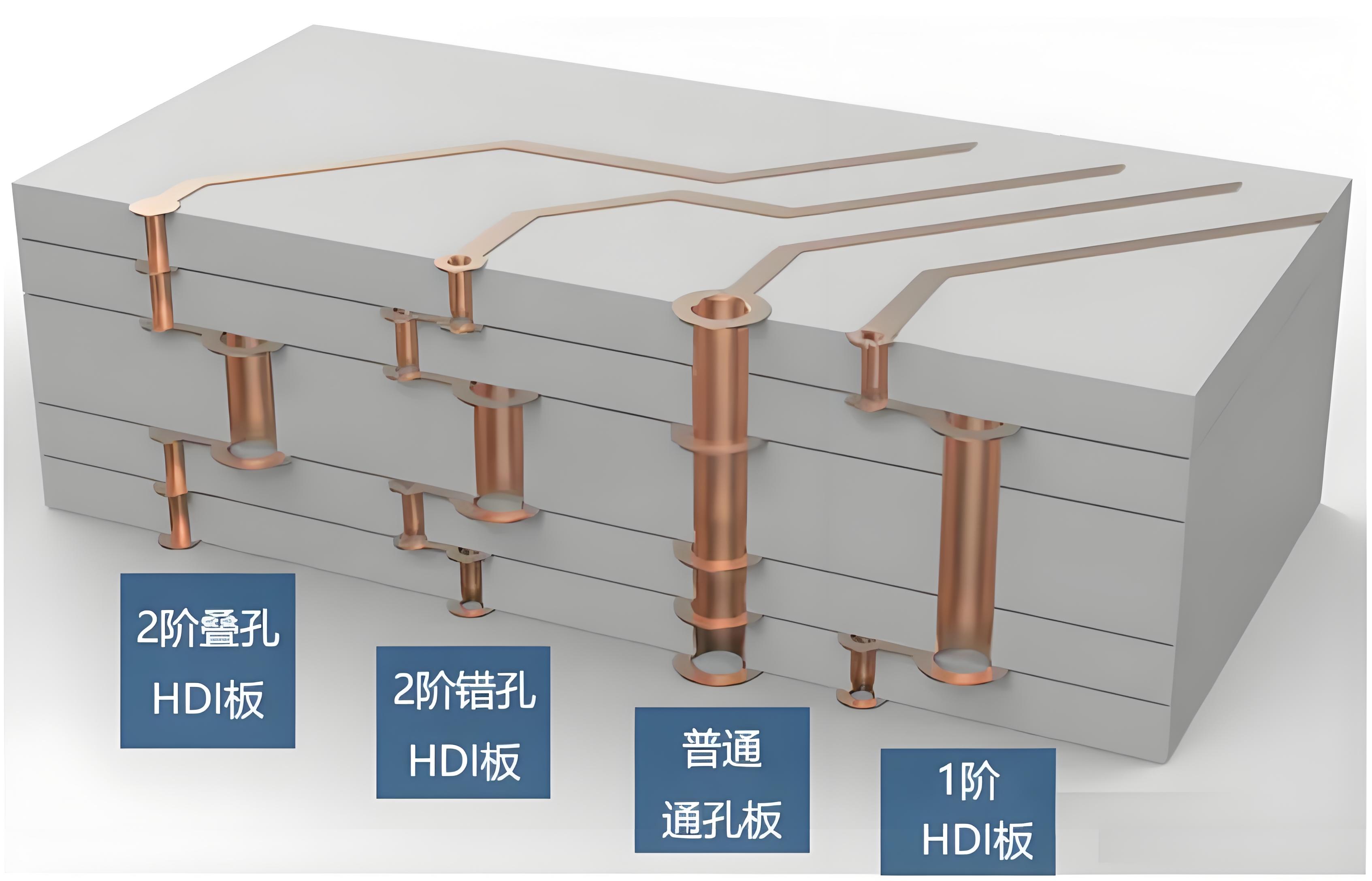
2. Core Value of Six-Layer HDI Stackup Design
Stackup design is a pivotal factor throughout the HDI PCB development process, directly determining electrical performance, manufacturability, and cost competitiveness. A well-considered stackup scheme systematically optimizes impedance control, signal integrity (SI), thermal management, and mechanical reliability. In today’s increasingly cost-competitive landscape of smart terminals and consumer electronics, stackup selection directly impacts a product’s overall cost-performance ratio. For the widely adopted six-layer HDI board, achieving the optimal balance among process complexity, performance level, and manufacturing cost has become a key focus in PCB design optimization.
Currently, mainstream six-layer HDI stackup solutions—covering both first-order and second-order types—can be categorized into three main types, each differing significantly in process flow, fabrication difficulty, and cost. These are analyzed individually below.
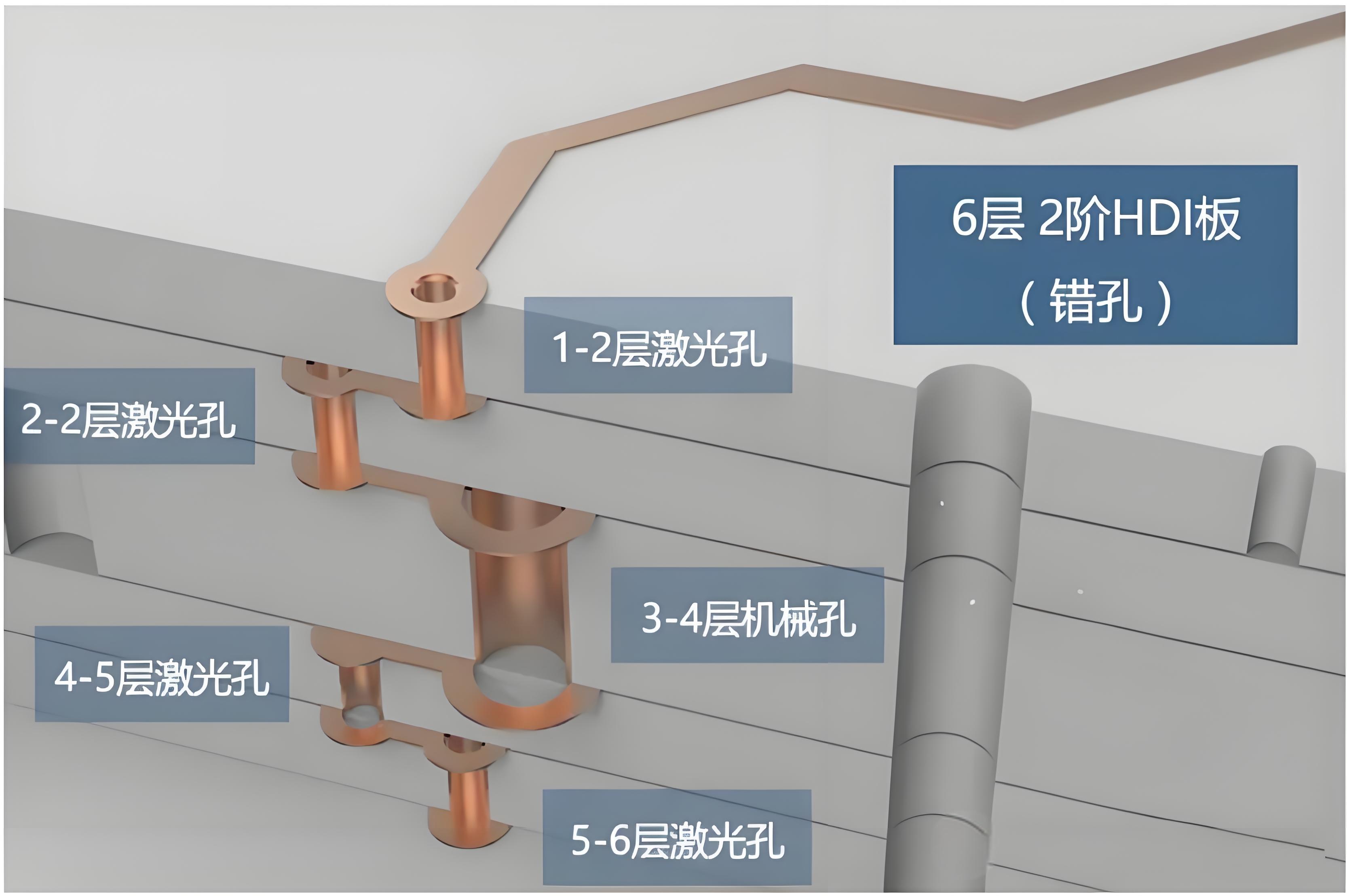
3. Detailed Analysis of Mainstream Six-Layer HDI Stackup Structures
Basic Six-Layer First-Order HDI – Single Lamination, 1+4+1 Structure
This solution adopts a 1+4+1 stackup architecture, where the inner core layers contain no buried vias, and the entire board requires only a single lamination step. Its fabrication process closely resembles that of a standard six-layer multilayer board, with the addition of only a few precision steps such as laser drilling of blind vias and plating/filling processes, resulting in a streamlined and efficient workflow.
In terms of material configuration, layers 2–3 and 4–5 can each be paired as two separate core laminates, with prepreg sheets and copper foil added on the outer layers. The full board is then bonded through a single lamination cycle, eliminating the need for multiple laminations or buried via processing.
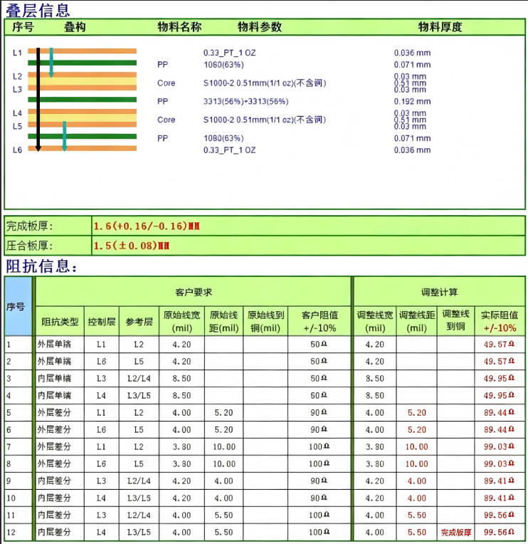
Key Advantages: Low process barrier, high production yield, short lead time, and the lowest manufacturing cost among all six-layer HDI options—offering outstanding cost-effectiveness.
Limitations: No internal buried vias; interlayer connections rely solely on surface blind vias and through-holes, resulting in lower routing flexibility compared to designs incorporating buried vias.
Typical Applications: General consumer electronics, standard industrial control boards, and high-volume production projects—making it the preferred choice for cost-sensitive designs.
Standard Six-Layer First-Order HDI – Double Lamination, 1+4+1 Structure (with Buried Vias)
This structure also follows the 1+N+1 (N=4) design principle, featuring a 1+4+1 stackup, but integrates buried vias within the inner core layers, requiring a double lamination process. The board incorporates a hybrid network of both blind and buried vias, significantly enhancing interlayer routing density and connection reliability compared to the basic version.
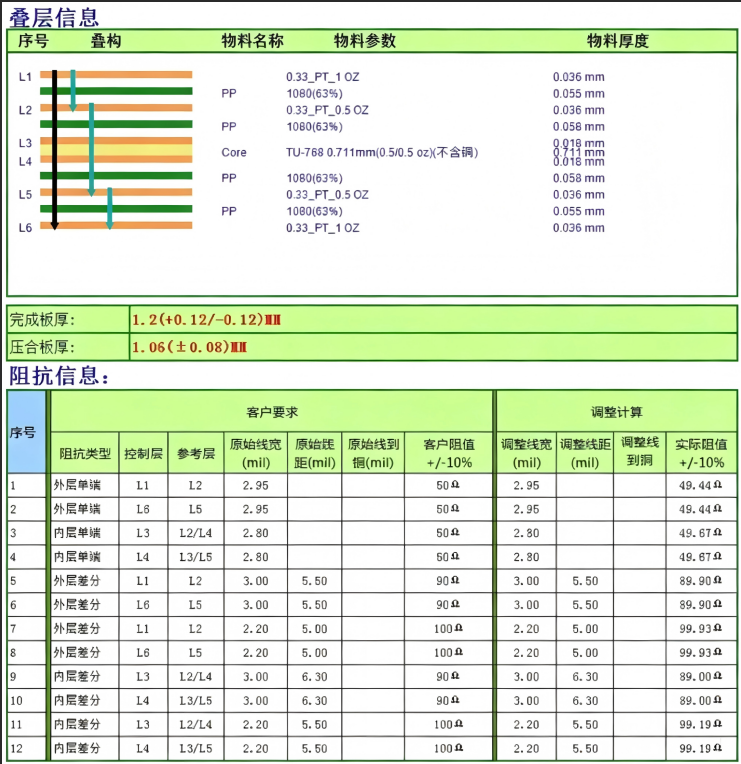
Key Advantages: The combination of blind and buried vias enables higher routing density and more stable signal transmission. The process is mature, with robust mass-production support across the industry.
Limitations: Requires double lamination, increasing process steps and extending production lead time. Manufacturing costs are notably higher than the basic version, with more stringent process control requirements.
Typical Applications: Mid-to-high-end consumer electronics, compact high-speed signal devices, and standard premium products with explicit high-density routing requirements.
Design Optimization Tip: When electrical performance and structural constraints meet design specifications, consider optimizing a standard first-order HDI with buried vias into a simplified single-lamination structure without buried vias. This approach significantly reduces processing complexity and material costs without compromising basic functionality—a common cost-reduction strategy in current industry practice.
Non-Standard Six-Layer Second-Order HDI – Double Lamination, 1+1+2+1+1 Structure (Interlayer Blind Vias)
This solution belongs to second-order HDI, adopting a 1+1+N+1+1 (N=2) architecture, resulting in an overall 1+1+2+1+1 stackup requiring double lamination. Its defining feature is support for 1-to-3 layer interlayer blind vias, with blind via depth twice that of standard 1-to-2 layer vias, significantly increasing interlayer connectivity span.
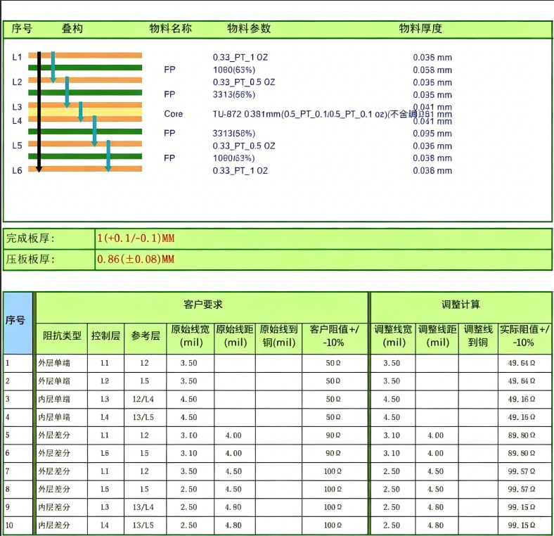
This structure imposes strict design constraints: 1-to-3 interlayer blind vias cannot be replaced by stacked 1-to-2 and 2-to-3 vias, giving it high design uniqueness.
Process Challenges: Deep interlayer blind vias demand extremely high precision in laser drilling and exceptional via wall quality. During subsequent electroless copper deposition and plating/filling steps, achieving uniform copper thickness in deep vias is difficult, often leading to copper voids or poor conductivity. Only a limited number of PCB manufacturers with advanced process capabilities can achieve stable mass production.
Overall Assessment: Extremely high process difficulty, low yield, high cost, and unpredictable delivery timelines—this option is not recommended unless absolutely necessary.
Typical Applications: Exclusively reserved for specialized, high-end custom products with mandatory interlayer connectivity requirements.
Optimization Recommendation: If design permits, replace interlayer blind vias with a first-order stacked via approach (1-to-2 + 2-to-3 combination) to substantially reduce process risk and cost.
Six-Layer AnyLayer HDI – Ultra-High-Density Interconnect
AnyLayer HDI enables direct blind via interconnection between any layers, without fixed layer restrictions. It offers the highest routing freedom, integration density, and signal integrity among all six-layer HDI types. This structure employs sequential build-up processing with multiple laser drilling and plating steps, representing the highest level of process complexity and cost in six-layer HDI technology.
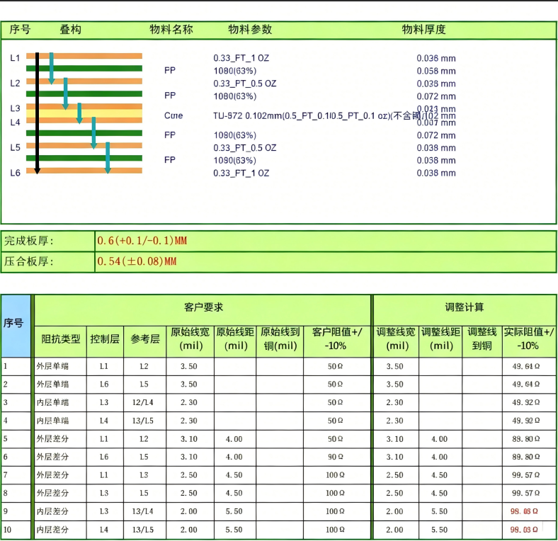
Typical Applications: High-end precision instruments, high-frequency/high-speed communication equipment, and flagship wearable devices—products demanding extreme performance. Rarely used in general consumer electronics.
Comparison and Selection Summary of Six-Layer HDI Stackup Structures
4.1 Comparison of Advantages and Disadvantages
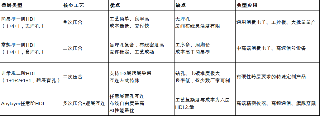
Core Principles for Stackup Selection
General Mass-Production Scenarios – Prioritize the basic single-lamination six-layer first-order HDI to achieve the lowest total cost and highest production yield while meeting performance requirements.
Mid-to-High-End Standard Scenarios – Select the standard double-lamination six-layer first-order HDI (with buried vias) to fulfill high-density routing and signal quality needs using mature, reliable processes.
Special Custom Scenarios – Use the second-order interlayer blind via HDI structure only when the product has non-negotiable interlayer connectivity requirements. During the design phase, always first evaluate whether a stacked via alternative can be adopted to mitigate risks.
High-End High-Frequency/High-Speed Scenarios – Select AnyLayer HDI as needed to fully leverage its routing freedom and signal integrity advantages, while accepting its high cost and extended lead times.
Conclusion: Six-layer HDI stackup design represents a delicate balance among performance, manufacturability, and cost. Design engineers should engage in stackup selection during the early stages of product specification definition, making informed trade-offs based on electrical requirements, production volume, and supplier process capabilities to achieve optimal engineering outcomes.
trending news
Contact Us