



Sorry, no sales person is available right now to take your call. Pls leave a message and we will reply to you via email as soon as possible.
Home/ PCB News/ AI Computing Power Consumption Surges—Why Ceramic Substrates Are the "Ultimate Armor" for AI Chip Thermal Management?
AI Computing Power Consumption Surges—Why Ceramic Substrates Are the "Ultimate Armor" for AI Chip Thermal Management?
2026-07-01
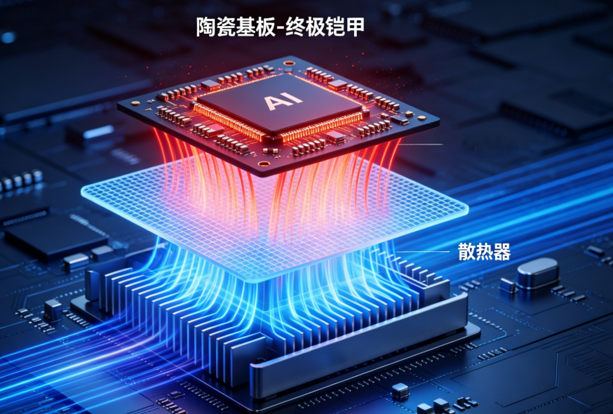
The global AI computing power race has fully entered a high-power-density iteration cycle. Thermal management has evolved from an auxiliary aspect of traditional packaging into a core bottleneck that constrains the release of high-end AI chip performance, operational reliability, and overall system lifecycle. With the deployment of next-generation high-performance chips such as NVIDIA’s H100 and B200, single-chip power consumption has surged from 700W to over 1000W, while the next generation of flagship AI chips is targeting power levels of 1500W and beyond. Concurrently, the power density per rack in AI servers has skyrocketed from the traditional tens of kilowatts to over 600 kilowatts. This exponential growth in computing power and power consumption has driven a quantum leap in heat flux density at the package level, completely surpassing the physical performance limits of conventional packaging substrates like FR-4 organic boards and standard glass substrates. Substrate innovation for high-power scenarios has thus become an inevitable industry trend.
The central challenge in thermal management for kilowatt-class AI chips lies in insufficient ultra-high heat flux conduction capability and poor thermal stress compatibility in packaging. Traditional substrates easily lead to hotspot concentration, junction temperature exceeding limits, forced frequency throttling, and interlayer delamination failures—significantly reducing effective computing output and equipment service life. Against this industrial backdrop, ceramic substrates—long used in high-reliability applications such as power semiconductors and aerospace/defense—have rapidly crossed over into AI applications. Thanks to their excellent thermal conductivity, coefficient of thermal expansion (CTE) closely matched to silicon, and high structural rigidity, ceramics have transitioned from niche specialty materials to essential substrates for ultra-high-power AI packaging.
I. Core Material Mechanisms: Three Intrinsic Properties of Ceramic Substrates Address AI Packaging Thermal Challenges
The industrial value of ceramic substrates stems from their intrinsic physicochemical properties precisely aligning with three core engineering requirements of ultra-high-power AI packaging: thermal conduction, thermal stress buffering, and structural stability. Baineng Yunban, a domestic leader in precision PCBs, has established a full portfolio of ceramic substrates—including aluminum nitride (AlN), silicon nitride (Si₃N₄), and alumina (Al₂O₃)—and mastered mass-production processes across HTCC, LTCC, and AMB technologies. The company now enables scalable manufacturing and customized development of 1–6 layer high-precision ceramic PCBs, fully unlocking the practical value of ceramic substrates.
Orders-of-Magnitude Thermal Conductivity Advantage Significantly Reduces Interfacial Thermal Resistance
The primary cause of thermal failure in high-end AI chips is not overall temperature rise, but localized hotspot accumulation due to ultra-high heat flux density. Traditional FR-4 organic substrates, with a thermal conductivity of only 0.3 W/m·K, exhibit extremely poor in-plane and through-thickness heat spreading capabilities, resulting in persistently high interfacial thermal resistance. Faced with AI chip heat flux densities reaching hundreds of watts per square centimeter, FR-4 cannot rapidly dissipate concentrated heat, causing rapid junction temperature overshoot and triggering TDP-based power throttling and performance degradation.
Ceramic substrates deliver generational leaps in thermal performance: aluminum nitride (AlN) achieves thermal conductivity of 170–230 W/m·K—hundreds of times higher than FR-4. Its dense, pore-free structure enables low-loss vertical heat conduction pathways, making it the preferred substrate for 1000W+ ultra-high-power AI chips. Commercially available silicon nitride (Si₃N₄) maintains stable thermal conductivity between 20–90 W/m·K, with high-purity lab samples exceeding 100 W/m·K, well-suited for mid-to-high-power computing scenarios.
Baineng Yunban’s proprietary AlN ceramic substrate solution achieves a peak thermal conductivity of 230 W/m·K. Through thick copper integration and stepped structural optimization, it further enhances vertical heat flow paths, effectively reducing both overall package thermal resistance and interfacial contact resistance. This enables sustained, full-load operation of 1500W-class chips under steady-state conditions, fundamentally eliminating heat accumulation and performance degradation under heavy workloads.
Silicon-Matched CTE Mitigates Thermal Cycling Fatigue Failures
AI servers operate under harsh conditions involving frequent power cycling and large temperature swings. Mismatch in coefficient of thermal expansion (CTE) within the packaging system is the primary structural cause of solder joint fatigue, substrate warpage, interlayer delamination, and packaging failure. Differential thermal deformation between the substrate and silicon chip accumulates cyclic thermal stress during repeated heating and cooling, eventually leading to microcrack propagation, solder joint fracture, and catastrophic package failure.
Silicon chips have a CTE of approximately 3 ppm/°C, while ceramic substrates maintain a stable CTE range of 3–9 ppm/K. This close match ensures highly coupled deformation behavior, significantly offsetting interfacial thermal stress during temperature transitions and preventing thermal cycling fatigue failures. In contrast, traditional organic substrates exhibit wide CTE variations and poor stability, resulting in severe mismatch with silicon chips and rendering them unsuitable for the long-duration, high-frequency, high-reliability operating conditions of AI systems.
High-Modulus Structural Properties Enhance Dimensional Stability Under Extreme Conditions
Ceramic materials exhibit Young’s moduli of 50–90 GPa, offering inherent advantages in high rigidity, deformation resistance, high-temperature tolerance, and vibration resistance. Under the extreme operating conditions of AI servers—high load, high humidity, and long service life—ceramics maintain dimensional accuracy over time, eliminating packaging misalignment and interlayer failures caused by structural deformation.
Baineng Yunban’s AMB (Active Metal Brazing) thick-copper process achieves atomic-level metallurgical bonding between the ceramic body and copper conductive layers, completely eliminating interlayer voids and delamination defects. The resulting products withstand thermal shock cycles from -40°C to 150°C, significantly enhancing power cycling reliability and extending overall system service life to meet stringent high-reliability standards for computing infrastructure.
II. Key Application Scenarios: Essential Adoption in High-Performance Computing and High-Speed Optical Modules
As AI chip power density continues to rise and optical modules advance toward ultra-high speeds, traditional substrates can no longer simultaneously satisfy thermal, high-frequency signal integrity, and reliability requirements. Ceramic substrates have shifted from performance-enhancing options to essential components, achieving scaled adoption in two core domains: high-performance computing chip packaging and ultra-high-speed optical modules, driving continuous industrial growth.
Advanced Packaging for High-Performance GPU/ASIC Chips
Unlocking the full performance potential of kilowatt-class AI chips depends on low-resistance vertical thermal architectures. Integrating ceramic substrates into HDI hybrid packaging structures creates efficient vertical heat dissipation channels, resolving hotspot concentration under ultra-high heat flux and preventing performance throttling. Baineng Yunban’s AI-optimized ceramic substrate solution is compatible with advanced HDI precision hybrid packaging processes, balancing high-precision microvia routing with ultra-low thermal resistance to enable lossless, stable computing output.
Moreover, while advanced packaging approaches like CoWoS adopt “substrate-less” architectures to enhance interconnect density, they suffer from structural weaknesses such as stress concentration, which can cause solder joint cracking and silicon micro-damage, impacting yield. Ceramic substrates serve as highly effective stress-buffering layers, distributing concentrated stresses during packaging and operation, thereby addressing reliability gaps in advanced packaging and significantly improving chip yield and long-term operational stability.
800G/1.6T Ultra-High-Speed Optical Modules
In the evolution toward 800G and 1.6T optical modules, both photonic/electronic chip power density and signal bandwidth have doubled. High-frequency dielectric losses and localized chip heating have become critical bottlenecks limiting performance and reliability. Aluminum nitride ceramic substrates uniquely combine ultra-high thermal conductivity, low dielectric loss, and high insulation voltage, simultaneously addressing high-speed signal transmission and high-density thermal dissipation challenges—perfectly aligning with trends toward miniaturization, high bandwidth, and high power in optical modules.
From a value perspective, the application-driven value of ceramic substrates continues to rise: a single 800G optical module incorporates approximately 12 ceramic substrates; upgrading to 1.6T increases the per-module substrate value from $17 to $22. Even with silicon photonics optimizing substrate usage, the per-unit value continues to climb. Baineng Yunban’s low-dielectric-loss processing and ultra-high-precision fabrication ensure low-loss high-frequency signal transmission while enabling efficient thermal spreading for photonic chips, precisely meeting the demands of next-generation optical modules.
III. Industry Bottlenecks: Cost, Brittleness, and Yield Constraints Limit Mass Adoption
Ceramic substrates represent the optimal engineering solution for ultra-high-power AI applications today. However, due to inherent material properties and demanding precision manufacturing processes, three key constraints—high cost, brittleness, and limited yield—hinder their widespread adoption, restricting current use primarily to premium, high-reliability computing segments.
First, high-end substrate costs present a significant barrier. Aluminum nitride ceramic substrates cost 5–10 times more than traditional organic substrates and are also more expensive than glass substrates. While the current tight supply-demand balance for high-end AI chips allows the industry to pay a premium for superior thermal performance, persistently high costs remain the main obstacle to adoption in mid-to-low-end computing segments and large-scale deployment.
Second, inherent material brittleness limits large-format applications. Ceramics are naturally brittle and impact-sensitive. Large-size substrates are prone to cracking and chipping during processing, and yield control difficulty increases exponentially with substrate size, making them unsuitable for large-panel, high-volume manufacturing scenarios.
Third, ultra-precision microvia processing suffers from low yields. The extreme hardness of ceramic materials causes severe wear on conventional mechanical drilling tools, while laser drilling often induces edge microcracks and hole wall defects. The industry’s mainstream hybrid process—combining mechanical micro-drilling, laser ablation, and chemical etching—operates within narrow parameter windows and is difficult to control. Currently, the overall production yield for aluminum nitride ceramic substrates is only 70%–80%, far below the mature >95% yield levels of organic substrates.
To address these industry-wide process challenges, Baineng Yunban has upgraded its end-to-end manufacturing process, introducing high-precision micro-drilling equipment and closed-loop laser energy control systems, complemented by a comprehensive DFM (Design for Manufacturability) framework. This approach precisely avoids microvia defects and suppresses microcrack formation, steadily narrowing the yield gap between ceramic and traditional substrates, while supporting multi-specification, high-precision customization to meet diverse AI computing demands.
IV. Technology Roadmap Analysis: Glass and Ceramic Substrates Are Complementary, Not Competitive
The long-standing debate between glass and ceramic substrate roadmaps stems from their distinct technical positioning and application scenarios. Rather than being substitutes in competition, they are complementary and co-evolving solutions that jointly replace traditional organic substrates to meet the diverse needs of AI packaging.
Glass substrates dominate high-density, high-frequency interconnect applications, excelling in low signal dielectric loss, ultra-fine precision routing, large-format monolithic forming, and excellent CTE matching with silicon chips. They are ideally suited for CPO (Co-Packaged Optics), high-speed signal transmission, and other scenarios prioritizing signal integrity and interconnect density.
Ceramic substrates lead in high-power thermal management and high-reliability packaging, leveraging unmatched advantages in ultra-high thermal conductivity, low thermal stress deformation, and high structural rigidity. They are uniquely suited for high-power-density, high-reliability applications such as premium GPUs, high-power ASICs, and high-speed optical modules—making them irreplaceable substrates for ultra-high-power computing systems.
Kyocera’s April 2026 multi-layer ceramic substrate test data further validates that, in ultra-high-power computing scenarios, ceramic substrates comprehensively outperform glass substrates in thermal efficiency, thermal cycling reliability, and structural stability—solidifying their dominant position in high-power applications. Baineng Yunban, with its advantages in localized rapid delivery, cost-effective customization, and fully autonomous process control, effectively addresses domestic capacity gaps in high-end ceramic substrates and accelerates China’s import substitution progress.
From a long-term industry perspective, future AI chip performance bottlenecks will gradually shift from thermal constraints to high-density interconnect limitations, giving glass substrates broader long-term growth potential. However, over the next 3–5 years, rising chip power density remains the industry’s core challenge, ensuring ceramic substrates maintain clear market leadership in terms of growth momentum and deployment certainty.
V. Industry Summary and Outlook: Ceramic Substrates Define a New Paradigm for High-Power AI Thermal Management
As AI chip power consumption breaks through the kilowatt barrier and approaches 2000W levels, traditional organic and glass substrates have reached their physical limits in thermal management and reliability, unable to support continued high-end computing advancement. Drawing on decades of technological maturity from aerospace and power semiconductor applications, ceramic substrates—thanks to their irreplaceable thermal and reliability performance—have undergone a strategic value leap in the AI computing wave, becoming the ultimate thermal armor safeguarding stable operation of ultra-high-power chips.
From a technology evolution standpoint, ceramic substrates represent the optimal engineering solution for the current ultra-high-power AI era—but not the final form. As computing density continues to rise and packaging architectures evolve, thermal materials and processes will keep advancing. Future progress in yield improvement, cost reduction, and multi-layer precision manufacturing will define the upper limits of the AI thermal management industry.
Domestic leaders like Baineng Yunban are deeply investing in end-to-end ceramic substrate process innovation, continuously refining precision manufacturing and customized solutions. This empowers China’s AI hardware ecosystem to overcome high-end thermal bottlenecks, break foreign monopolies, and strengthen the core competitiveness of the domestic supply chain in the critical arena of computing power versus thermal management—securing strategic initiative in the industry’s future development.
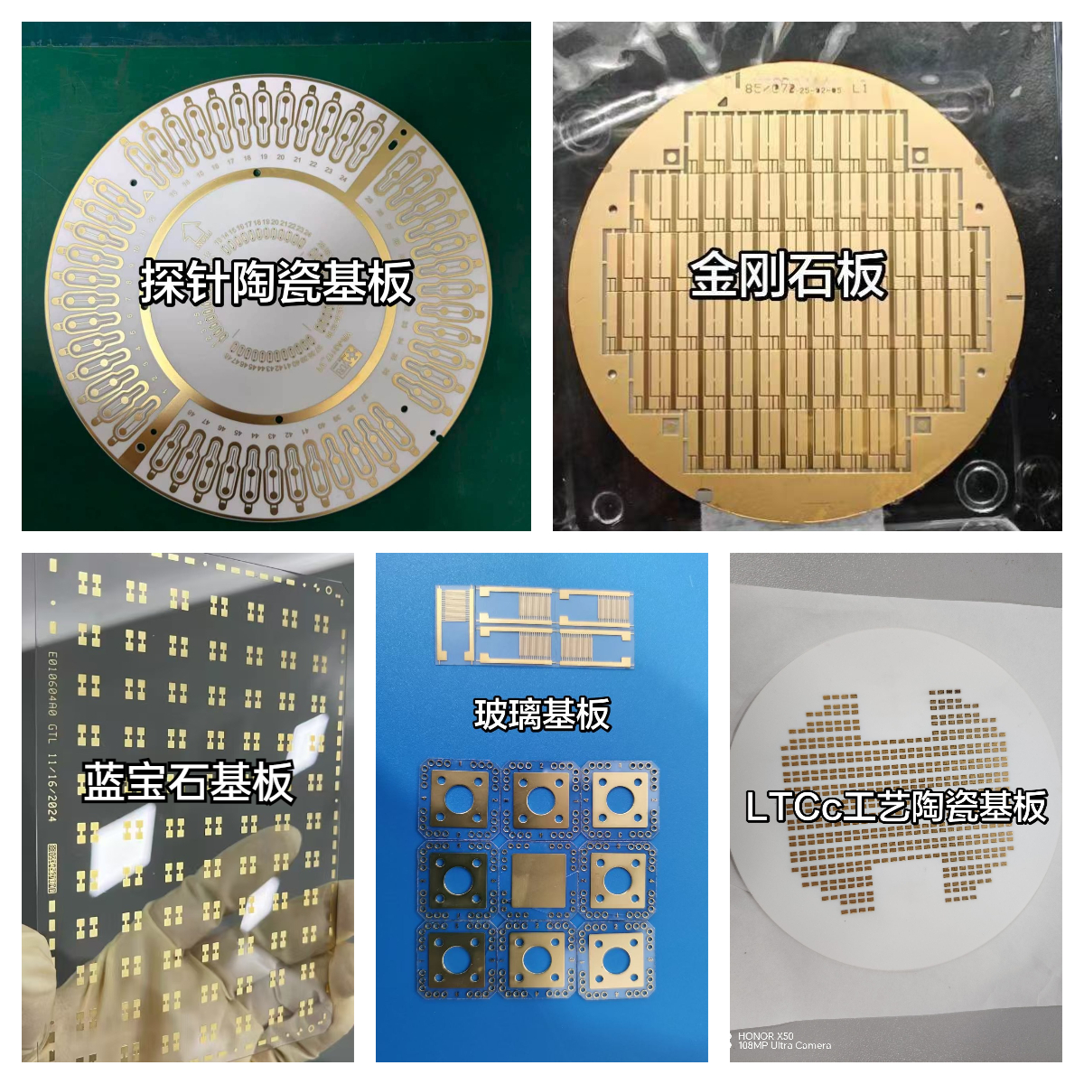
Product showcase of Baineng Yunban: ceramic substrates, glass substrates, diamond substrates, and more
trending news
Contact Us