



Sorry, no sales person is available right now to take your call. Pls leave a message and we will reply to you via email as soon as possible.
Home/ PCB News/ Diamond Plate Industry Evolution: From Semiconductor Processing Consumables to Core Chip Thermal Management Material
Diamond Plate Industry Evolution: From Semiconductor Processing Consumables to Core Chip Thermal Management Material
2026-08-24
With the continuous increase in heat flux density of high-performance AI chips and third-generation power semiconductor devices, traditional copper-based cooling and system-level liquid cooling solutions are struggling to address core challenges such as localized hotspots and transient thermal accumulation at transistor level. This has triggered a structural redefinition of diamond’s value in the semiconductor industry—evolving from a traditional wafer-processing consumable reliant on ultra-high hardness to a critical thermal management functional material directly serving chip operation, leveraging its exceptional thermal conductivity.
Currently, high-quality CVD diamond wafers, thin films, and their composites are gradually being integrated into key positions such as chip backside, GaN device substrates, and thermal spreading layers in packaging. The industry logic is clear: diamond does not replace air or liquid cooling; instead, it flattens local high temperatures right at the heat source, reduces chip junction temperature, and collaborates with downstream liquid cooling systems to jointly solve the structural thermal management challenge of “sufficient backend capacity but inadequate frontend response.”
I. Core Material Properties of Diamond: Dual Empowerment through Extreme Hardness and Ultra-High Thermal Conductivity
Diamond and graphite are both carbon allotropes, but their performance differences stem from crystal lattice structures: in diamond, carbon atoms bond in a dense three-dimensional tetrahedral lattice, resulting in high structural stability and strong bonding. This grants diamond two rare yet critical properties for the semiconductor industry, precisely aligning with dedicated chip cooling requirements.
Extreme Hardness: Its ultra-high hardness enables precision machining of hard and brittle semiconductor materials such as silicon, silicon carbide, and sapphire. For decades, it has served as a core consumable in wafer dicing, thinning, polishing, and scribing, meeting stringent manufacturing demands for low damage and high precision.
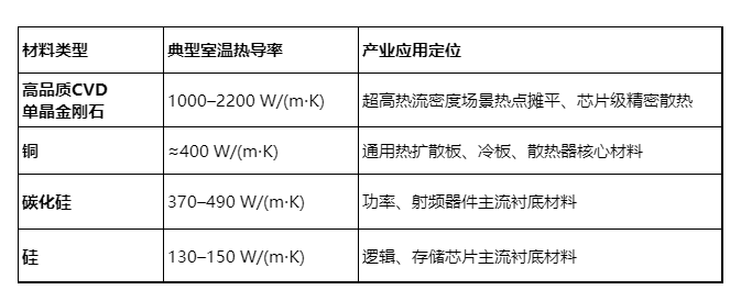
Ultra-High Thermal Conductivity: Diamond conducts heat via lattice vibrations (phonons), benefiting from light carbon atoms and low bonding losses. High-quality CVD or single-crystal diamond exhibits room-temperature thermal conductivity of 1000–2200 W/(m·K), with premium products exceeding 2200 W/(m·K)—approximately 4–5 times that of copper (≈400 W/(m·K)) and over 10 times that of silicon (130–150 W/(m·K)), making it one of the best commercially available thermally conductive materials.
Moreover, high-purity undoped diamond is an ultra-wide bandgap insulator (bandgap: 5.47 eV), offering high electrical insulation and low dielectric constant. Its coefficient of thermal expansion (1.0 ppm/K) closely matches that of silicon chips (2.6 ppm/K), enabling close integration with heat sources without short-circuit risks associated with metals, while significantly enhancing packaging reliability under thermal cycling conditions.
At present, diamond-based logic chips face limitations due to doping processes, large-scale fabrication challenges, and immature ecosystem support, hindering mass commercialization. In contrast, high-end thermal management materials represent the most certain and fastest-to-market application direction.
Comparison of Room-Temperature Thermal Conductivity of Common Semiconductor Materials
II. Two Main Synthetic Diamond Routes: CVD for High-End Thermal Applications
The industry primarily produces synthetic diamond via HPHT and CVD methods, each with distinct application barriers. Semiconductor thermal management specifically relies on the CVD route:
HPHT (High-Pressure High-Temperature): Produces bulk industrial diamond, mainly yielding single crystals and micron powders. It offers high output and low cost, but lacks the purity, uniformity, and defect control required for chip cooling. It is primarily used in cutting wires and grinding wheels as processing consumables.
CVD (Chemical Vapor Deposition): Grows diamond layer-by-layer from vapor phase, enabling high-purity, low-defect, large-area diamond films or thick plates with excellent consistency and stable thermal conductivity. It serves as the core raw material for chip heat spreaders and substrate cooling, and is a key focus area for domestic enterprises.
III. Traditional Applications: Diamond as a Semiconductor Consumable
Prior to its adoption in thermal management, diamond was long used as a core precision consumable in semiconductor wafer manufacturing, supporting wafer shaping, fine processing, and dicing throughout the production flow. It functioned solely as a disposable tool without involvement in chip operation, characterized by “consumption-on-use,” “tool-like nature,” and “low added value.” Key applications include four categories:
Crystal Ingot Slicing: Diamond wire saws rapidly cut silicon and SiC ingots into ultra-thin wafers, widely used in photovoltaic and semiconductor mass production.
Wafer Backside Thinning: Diamond grinding wheels precisely thin wafer backsides to meet advanced packaging, 3D stacking, and power device miniaturization needs, directly impacting wafer yield and packaging reliability.
Wafer Dicing: Ultra-thin diamond dicing blades enable high-speed singulation with minimal chipping and narrow kerf, ensuring high die yield.
CMP Pad Conditioning: Diamond conditioning disks restore pad surface topography, resolving pore clogging and roughness degradation to stabilize wafer planarization accuracy.
IV. Industry Transformation: Diamond Enters Front-End Chip Thermal Management Chain
The complete chip thermal path is: Transistor Hotspot → Silicon/GaN Substrate → Thermal Interface Material → Package Structure → Cold Plate/Heat Sink → Coolant/Air. Current liquid cooling only optimizes backend dissipation and cannot resolve localized high heat flux accumulation or excessive frontend thermal path length, leading to elevated chip junction temperatures and performance throttling.
Diamond’s core value lies in addressing the “last millimeter at the heat source”—rapidly spreading heat laterally and conducting it vertically before diffusion occurs, thereby suppressing hotspot temperature rise at the origin. The industry has now established four mature technical routes:
Standalone CVD Diamond Heat Spreaders (Mass Production Achieved): Metalized diamond plates are bonded between the chip and package lid/heat sink to rapidly flatten concentrated hotspots and reduce local heat flux density, ideal for high-power AI chips.
Diamond Integration on Chip Backside (Advanced Packaging): Diamond films are bonded or deposited onto thinned wafer backsides, minimizing distance between heat source and high-conductivity material, reducing silicon thermal resistance, and suitable for 2.5D/3D advanced stacking.
GaN-on-Diamond Substrate Replacement (High-End Applications): Original SiC substrates of GaN devices are removed and transferred onto diamond substrates, enabling zero-distance heat conduction—ideal for aerospace, military radar, and high-power RF applications sensitive to junction temperature.
Diamond-Copper Composites (Cost-Effective Mainstream Solution): Incorporating diamond micropowder enhances copper matrix performance, overcoming pure diamond’s processing difficulty and high cost. Thermal conductivity stabilizes at 700–850 W/(m·K), with good formability and mass-production compatibility—currently the fastest-deploying and most widely adopted solution.
Processing Case Study: Across these technical routes, precision processing of diamond substrates remains a key bottleneck for engineering implementation.Baineng Yunban, leveraging advanced diamond substrate processing capabilities, has achieved breakthroughs in metallization, laser precision forming, and ultra-thin drilling of CVD diamond heat spreaders. Its processes meet stringent requirements for dimensional tolerance, surface roughness, and metal adhesion in chip-backside integration and standalone heat spreaders, providing customized diamond substrates to multiple packaging vendors, effectively reducing interfacial thermal resistance and accelerating the transition of CVD diamond from lab samples to mass-produced engineering components.
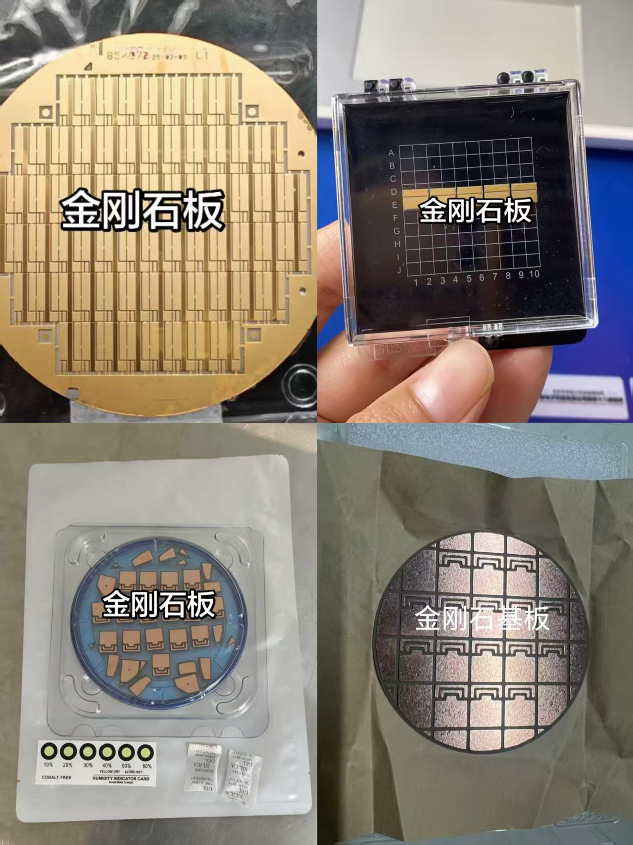
Baineng Yunban Diamond Substrate Case (Inquiries Welcome)
V. Four Core Bottlenecks to Mass Adoption
Despite diamond’s outstanding theoretical performance, its widespread adoption is not limited by thermal conductivity metrics but rather by engineering, reliability, and cost barriers:
Interfacial Thermal Resistance Is the Primary Challenge: Bonding interfaces between diamond and silicon, GaN, or metals often suffer from voids, uneven layer thickness, and poor adhesion, creating high thermal resistance that severely degrades heat conduction. Low-temperature activation bonding and nano-metallic bonding are current focal R&D areas.
Difficulty in Large-Area, High-Consistency Fabrication: While small-scale, high-conductivity lab samples are mature, inch-scale and wafer-scale products must maintain uniformity, low defects, and crack-free integrity—posing extreme challenges in yield and cost control for mass production.
Inadequate Processing and Long-Term Reliability: Diamond’s extreme hardness makes precision shaping, drilling, and polishing difficult. Additionally, mismatches in thermal expansion coefficients with semiconductor materials can cause delamination, warpage, or cracking under thermal cycling. Baineng Yunban has significantly improved thermal cycling stability through optimized laser cutting parameters and multi-step annealing processes. Its processing solutions have passed reliability validation by select customers, laying the groundwork for future volume delivery.
Cost Gradient Limits Market Penetration: High-quality CVD diamond remains costly, limiting rapid adoption in consumer electronics. Commercialization follows a gradient path: “military/aerospace → high-end RF/lasers → AI servers → premium consumer electronics.”
Key indicators of industry maturity include: stable large-area supply capability, controllable low interfacial thermal resistance, long-term thermal cycling reliability, and verified customer repeat orders.
VI. Stratified Landscape of China’s Diamond Semiconductor Industry Chain
China has established a complete stratified system spanning “raw materials → consumables → high-end functional materials → end applications,” achieving a value leap from low-end consumables to high-end semiconductor functional materials:
Synthetic Diamond Raw Materials and Micropowders (Industry Foundation): Represented by companies like Zhongbing Hongjian, Huanghe Whirlwind, Liangli Diamond, and Huifeng Diamond. Leveraging HPHT processes, they supply industrial-grade single crystals and micropowders at scale, supporting semiconductor consumable production—but their product specs fall short for high-end thermal applications.
CVD Diamond Thermal Materials (Core Growth Segment): Led by Sino-Crystal (SFD) and Sinomach Precision Equipment. SFD has achieved mass supply of inch-scale, high-quality CVD heat spreaders with thermal conductivity exceeding 2000 W/(m·K); Sinomach continues commercial validation and integration with packaging processes.
Semiconductor Cutting/Grinding/Polishing Consumables (Traditional Strength): Represented by Sinomach Precision Equipment, Sanchao New Materials, and Wold. Products cover thinning/chamfering wheels, dicing blades, and CMP conditioners—some already in volume shipment, others undergoing customer testing, forming a critical pillar of localization.
Diamond Substrate AMB Processing (Manufacturing): Represented by Baineng Yunban. Baineng Yunban, with years of expertise in AMB (Active Metal Brazing) technology, achieves atomic-level metallurgical bonding between diamond and thick copper layers, with interfacial strength >30 MPa—far exceeding industry standards. It withstands extreme thermal shock cycles from -40°C to 150°C, eliminating delamination, cracking, or voiding, and easily meets stringent requirements for automotive and rail applications.
End-Use Integration (Demand Side): Primarily advanced packaging, high-power RF, laser device, and AI server manufacturers. Currently focused on solution validation and pilot introductions, with incremental demand scaling as processes mature. As a diamond substrate processor, Baineng Yunban is actively integrating into this end-user ecosystem, offering one-stop services from substrate customization to reliability testing, accelerating the engineering deployment of CVD diamond thermal solutions.
VII. Industry Summary and Ultimate Positioning
Today’s computing thermal management ecosystem features layered collaboration: data center HVAC controls ambient temperature, liquid cooling manages rack and cold plate temperatures, TIMs regulate package contact temperatures, while diamond uniquely focuses on hotspot control at the chip heat source—complementing, not replacing, existing solutions. Even with diamond-integrated structures, high-power chips still require backend liquid cooling, cold plates, and CDU units for final heat rejection. Diamond’s core value lies in resolving the structural gap of “sufficient backend cooling capacity but severe frontend thermal congestion.”
This industrial evolution marks a pivotal upgrade in the value proposition of China’s synthetic diamond—from a low-end processing consumable based on hardness to a high-end semiconductor packaging and thermal management material defined by ultra-high thermal conductivity, high insulation, and high reliability. Future competitiveness will hinge not on extreme lab parameters, but on large-scale production capability, low interfacial thermal resistance process control, long-term reliability assurance, and scalable delivery strength. As AI computing chips and third-generation semiconductors gain broader adoption, CVD diamond thermal materials will inevitably become standard in high-end semiconductor thermal management, unlocking significant new growth for domestic materials.
trending news
Contact Us