



Sorry, no sales person is available right now to take your call. Pls leave a message and we will reply to you via email as soon as possible.
Home/ PCB News/ Embedded Heat Dissipation Technology of PCB Copper Pads and Copper Posts: Design Applications, Failure Risks, and Process Specifications
Embedded Heat Dissipation Technology of PCB Copper Pads and Copper Posts: Design Applications, Failure Risks, and Process Specifications
2026-08-13
In fields such as automotive electronics, RF communications, aerospace, high-density computing, and power electronics, electronic equipment continues to evolve toward miniaturization, higher power density, and longer service life with enhanced reliability. Consequently, localized heat flux density on PCBs has risen sharply. Traditional cooling methods, constrained by the thermal conductivity of base materials and structural limitations, can no longer meet the precise temperature control requirements of high-power components, becoming a critical bottleneck that restricts performance optimization and long-term stable operation of high-end equipment. Against this backdrop, embedded copper coin and copper pedestal/pillar thermal management technologies—featuring ultra-low thermal resistance, structural integration, and compatibility with high-end mass production—have become benchmark solutions for localized thermal management in advanced PCBs.
Conventional FR-4 substrates exhibit thermal conductivity of only 0.2–0.4 W/m·K; even modified high-thermal-conductivity laminates typically do not exceed 12 W/m·K. Industry-standard approaches such as thickened copper pours, thermal via arrays, and localized copper expansion are suitable only for low-to-moderate thermal loads. Under high localized heat flux conditions, the inherent thermal resistance of the substrate becomes a significant bottleneck, rendering conventional measures nearly ineffective. Pure copper, with thermal conductivity of 380–400 W/m·K, enables the creation of direct, low-loss vertical thermal pathways when solid copper coins or pedestals are embedded in high-heat regions of the PCB, fundamentally overcoming substrate limitations and efficiently channeling concentrated heat away from components.
Although core industry standards such as IPC-2221 and IPC-6012 do not yet include dedicated clauses specifically addressing embedded copper coins or pedestals, these metallic inserts—as integral parts of the PCB structure—must fully comply with existing general specifications and undergo stricter controls during design, manufacturing, and validation phases.
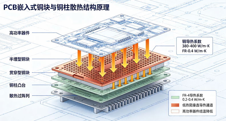
I. Design Applications
The core principle of embedded copper coin and pedestal structures lies in leveraging pure copper’s exceptional thermal conductivity (~380 W/m·K)—three orders of magnitude higher than that of FR-4 (~0.3 W/m·K)—to establish a direct, low-thermal-resistance vertical heat conduction path beneath high-heat-flux components such as MOSFETs, IGBTs, high-power LEDs, and RF power amplifiers, eliminating interfacial dielectric barriers. This structure rapidly transfers concentrated heat generated during operation from the PCB surface and inner layers to bottom-side thermal planes, external heat sinks, or chassis enclosures, effectively reducing component junction temperatures, mitigating high-temperature aging failures, and significantly enhancing operational reliability and service life across all operating conditions.
1.1 Core Thermal Dissipation Mechanism
Embedded copper structures replace low-conductivity FR-4 in localized areas with pure copper’s high bulk thermal conductivity, creating a low-impedance thermal pathway from heat source to heat sink. Their vertical heat transfer efficiency far surpasses conventional planar copper pours or via arrays, making them especially suitable for high-power scenarios with concentrated heat sources and steep thermal gradients.
1.2 Primary Design Types
Based on thermal load levels, mounting requirements, and thermal precision needs, the industry employs five mainstream embedded copper thermal structures, each offering distinct thermal characteristics and process challenges:
(1) Embedded Copper Coin
Solid copper coins are embedded within the substrate using multilayer lamination processes, categorized as semi-embedded or through-embedded:
Semi-embedded copper coin: One face is flush with the PCB surface while the other is buried within the board. Its flat profile supports standard SMT processes and is ideal for single-sided heat dissipation in double-sided high-power boards.
Through-embedded copper coin: Spans the entire PCB thickness, forming an unobstructed vertical thermal path with minimal thermal loss, specifically designed for thick boards and ultra-high localized heat flux applications.
This structure is widely used in high-layer-count precision boards, high-power RF circuits, and automotive power electronics, significantly enhancing local thermal performance without altering board外形, and offers strong mass-production compatibility.
(2) Surface-Mounted Copper Pedestal
Copper pedestals are micro-raised 3D thermal structures on the board surface that completely eliminate the FR-4 dielectric layer between component thermal pads and the heat spreader, minimizing contact thermal resistance. They offer superior ultimate thermal performance compared to embedded coins and can directly interface with component thermal pads, external heat sinks, or liquid cooling connectors, making them the preferred choice for ultra-low thermal resistance and high-precision thermal management. However, their complex fabrication, stringent dimensional tolerances, and high demands on coplanarity, solder paste volume, and reflow profile matching make them susceptible to voids and cold solder joints due to process deviations, limiting their use to high-end precision applications.
(3) Thermally Isolated Copper Base Pedestal
This design physically separates electrical circuitry from thermal pathways using independent copper pedestals, eliminating electrical crosstalk and achieving near-zero thermal resistance with effective thermal conductivity approaching that of pure copper (380 W/m·K). Mandatory design rules include: pedestals must be electrically isolated from any conductive traces, pads, or copper features; minimum feature size of 1 mm × 1 mm; and full connection of all thermal pedestals to the bottom-side solid copper base to ensure uninterrupted thermal paths. This structure is specifically engineered for high-power LEDs, COB optoelectronic devices, and other applications requiring high heat generation and precise thermal control, effectively addressing issues like luminous decay and thermal failure.
(4) Chip-Scale Copper Pillar Bump
An advanced packaging-level thermal solution, micro/nano-scale copper pillar bumps directly bond chips to substrates and can integrate thermoelectric materials for active temperature control, precisely addressing localized hot spots on chips. With extremely high dimensional accuracy and rapid thermal response, they are widely used in flip-chip packaging and high-end microelectronics, meeting dual demands for miniaturization and ultra-efficient cooling in consumer electronics and precision industrial equipment.
(5) Stepped Copper Coin Structure
Featuring a differential stepped cross-section, this design maximizes the ratio of heat dissipation surface area to substrate bonding area, optimizing thermal diffusion and conduction efficiency within limited space. Its compact form and strong resistance to thermal cycling make it ideal for miniature precision devices and aerospace applications where space is constrained and operating conditions are severe.
1.3 Application Scenarios and Solution Advantages
When localized heat flux density exceeds the capacity of conventional techniques—such as thickened copper, global copper pours, dense via arrays, or external heat sinks—and thermal simulation and prototype testing confirm that component junction temperatures remain above specification limits with high-temperature failure risks, embedded copper coin/pedestal solutions should be prioritized. Key application scenarios include:
Automotive Electronics: High-load, high-reliability components such as Engine Control Units (ECUs), high-power LED headlights, and Battery Management Systems (BMS);
Power Electronics: Energy storage inverters, high-power industrial power supplies, and IGBT modules with high current and heat dissipation;
RF Communications: 5G/6G base station RF power amplifiers and high-frequency antenna boards, simultaneously addressing signal integrity and localized overheating;
High-End Consumer Electronics: Core CPU/GPU thermal management in flagship laptops and smartphones, rapidly conducting heat to metal frames and back covers via embedded copper structures;
Aerospace and Defense: Airborne, spaceborne, and shipboard high-reliability systems operating under extreme thermal cycling and continuous duty cycles.
Compared to traditional approaches, embedded copper structures offer significant advantages: dense via arrays consume substantial routing resources and suffer from diminishing returns, while the substrate’s thermal resistance becomes a bottleneck under high heat; thermally conductive resin-filled vias are limited by material conductivity (only 7–10 W/m·K). In contrast, solid embedded copper directly replaces localized FR-4, drastically reducing thermal resistance and improving heat extraction efficiency by several to dozens of times, making it ideal for ultra-high heat flux conditions.
II. Failure Risks and Root Cause Analysis
Although embedded copper structures significantly enhance thermal performance, material property mismatches among copper, FR-4, and silicon chips, combined with specialized manufacturing processes, introduce multi-dimensional reliability risks. Based on industry mass-production failure cases and reliability test data, core failure modes and root causes can be categorized into nine types:
2.1 Thermo-Mechanical Stress Fatigue Failure (Primary Cause)
Mismatch in coefficients of thermal expansion (CTE) is the fundamental reliability concern: pure copper CTE is ~17×10⁻⁶/°C, FR-4 is ~14×10⁻⁶/°C, and silicon is only 2.6×10⁻⁶/°C. Under reflow soldering thermal shock, thermal cycling, and prolonged heating, inconsistent deformation generates cyclic stresses at copper-substrate interfaces, leading to irreversible damage over time. Typical failures include resin cracking, delamination, copper fracture, or inner-layer trace breaks at corners of large asymmetric copper features; interfacial debonding under frequent automotive thermal cycling; and chip cracking due to overstress at chip-scale copper pillar bumps. Mitigation strategies include optimizing fillet transitions and introducing low-CTE transition layers (e.g., Cu-Mo or Cu-W) to balance interfacial deformation and suppress crack initiation.
2.2 Lamination Process Defects
Embedded copper structures alter resin flow and wetting behavior of prepreg (PP), and improper parameters can cause hidden internal defects:
Interfacial Voids and Poor Adhesion: Improper slot dimensions, mismatched PP selection, or suboptimal lamination temperature/pressure/dwell time can prevent complete resin filling of gaps between copper and slot walls, resulting in resin starvation, bubbles, or poor bonding. These defects expand during thermal cycling and humidity aging, eventually causing delamination, insulation failure, or copper detachment. Tests show that when slot wall roughness Ra > 0.8 μm, void rate can reach 12.7%, with microcracks appearing after just 100 thermal cycles.
Resin Bleed-Out Contamination: Excessive resin overflow covering copper contact surfaces forms insulating layers, increasing contact thermal resistance and reducing solderability, leading to cold solder joints or thermal failure. Precision grinding and plasma cleaning are required for removal.
2.3 Drilling and Plating Process Defects
The significant hardness difference between copper inserts and FR-4 causes drill bit deflection, hole position deviation, rough hole walls, and copper chipping during drilling. Subsequent plating on rough surfaces results in uneven coating, weak adhesion, and cracks, delamination, or flaking, which can lead to open circuits under thermal cycling and vibration. Production requires optimized drilling parameters for copper-embedded zones and rigorous hole wall inspection with cross-sectional metallography sampling.
2.4 Excessive Board Surface Non-Flatness
Copper structure flatness and coplanarity directly impact SMT yield and thermal stability, with industry standards requiring flatness error ≤ ±50 μm. Protrusions disrupt coplanarity, causing cold solder joints; excessive recesses lead to insufficient solder paste fill and high void rates, resulting in poor thermal contact. Flatness defects stem from lamination deformation, uneven grinding, or board warpage, requiring end-to-end control across lamination, precision grinding, and surface treatment processes.
2.5 Stress-Induced Failure of Adjacent Plated Through Holes
Large embedded copper features alter local thermal fields and expansion behavior, subjecting nearby plated through holes (PTHs) and component holes to additional stress. In high-layer-count thick boards under frequent thermal cycling, this can cause plating cracks, corner fractures, or delamination, compromising interconnect reliability. Thermal-mechanical simulations during design should verify stress levels, ensuring a minimum clearance of ≥1.2 mm between copper structures and PTH edges to avoid stress concentration.
2.6 Localized Excessive Stiffness Causing Mechanical Stress Concentration
Solid copper inserts are much stiffer than FR-4, increasing local rigidity and altering overall board flexural behavior, making adjacent solder joints and traces stress concentration zones. Under combined vibration, shock, and thermal cycling—especially critical in aerospace and automotive applications—this can lead to solder joint cracks or trace fractures. Early-stage mechanical simulation is essential to optimize copper layout and balance board stiffness.
2.7 SMT Assembly Process Mismatch
Pure copper’s high thermal mass significantly disturbs local reflow temperature profiles, causing large differences in heating rates and peak temperatures between copper regions and standard substrate areas. This leads to head-in-pillow defects, poor solder wetting, voids, or solder slumping. Raised copper pedestals are especially sensitive to thermal disturbances, requiring tailored stencil apertures, solder paste volumes, and reflow profiles matched to copper’s thermal characteristics.
2.8 Progressive Degradation of Thermal Performance
Increasing Interfacial Thermal Resistance: Thermal interface materials (TIMs) degrade under high temperature/humidity and thermal cycling, drying out or phase-separating, which increases interfacial thermal resistance, reduces cooling efficiency, and causes continuous junction temperature rise until thermal runaway failure.
Copper Surface Oxidation and Corrosion: Unprotected exposed copper oxidizes rapidly in humid or salt-spray environments, forming low-conductivity oxide layers that impair radiative cooling and increase contact thermal resistance, progressively degrading thermal pathway performance.
2.9 Electrical Isolation and Insulation Failure
A common misconception is that thermal copper structures are exempt from electrical clearance rules. However, IPC-2221 conductor spacing and insulation thickness requirements fully apply to copper inserts. Insufficient spacing can lead to Conductive Anodic Filament (CAF) growth, dielectric breakdown, reduced insulation resistance, or excessive leakage current under prolonged operation, potentially causing short circuits and board burnout. This is a major cause of electrical failure in high-power PCBs and must be strictly avoided through compliant design.
III. Process Specifications and Key Control Points
PCBs with embedded copper coins/pedestals are structurally enhanced specialty boards requiring dedicated precision steps beyond standard multilayer processes, with comprehensive controls across design, manufacturing, assembly, and validation to balance thermal performance, manufacturability, and long-term reliability.
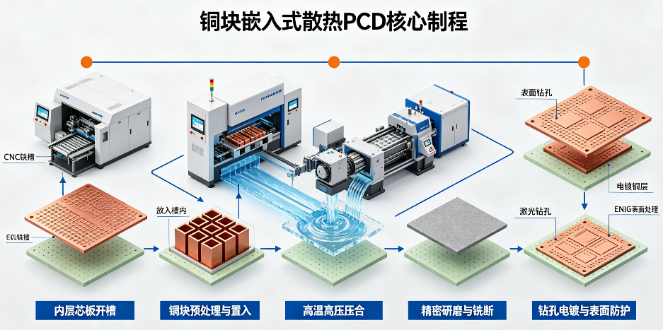
3.1 Core Process Flow
Based on mature mass-production practices, the standardized process is as follows (each step has dedicated control parameters):
Inner Layer Slot Milling and Prepreg (PP) Preconditioning: Precision CNC milling creates pre-embedding slots with XY tolerance ±0.15 mm, Z-depth tolerance ±0.1 mm, and slot wall roughness Ra ≤ 0.8 μm, leaving proper gap for resin fill; PP is simultaneously cut, dried, and dehumidified to prevent moisture-induced voids.
Copper Insert Pretreatment and Lamination: Copper inserts undergo polishing, degreasing, and anti-oxidation treatment, then are precisely placed into slotted cores. A dedicated lamination thermal-pressure profile with optimized dwell time ensures complete resin wetting and bonding, avoiding resin starvation, delamination, or misalignment.
Milling Separation and Precision Grinding: Electrically isolated embedded copper features are milled apart per circuit design; precision grinding removes resin bleed-out and height deviations, achieving flatness within ±50 μm to meet high-precision SMT requirements.
Differentiated Drilling and Plating: Drilling parameters are optimized for copper-embedded zones to prevent deflection and roughness; plating focuses on uniform coating at copper-substrate interfaces, eliminating sharp edges and thin spots.
Outer Layer Patterning and Surface Protection: Outer layer circuitry and solder mask are completed; exposed copper features receive protective finishes such as ENIG (Electroless Nickel Immersion Gold), electroless nickel-phosphorus, silver plating, or OSP to prevent oxidation, enhance solderability, and improve environmental resistance.
3.2 Key Design Rules
Based on IPC standards and production experience, four mandatory design rules are established:
Thermally Isolated Pedestals: Must be electrically isolated from all conductive features; minimum size ≥1 mm × 1 mm; all pedestals must connect fully to the bottom-side ground copper plane.
Plated Hole Isolation: When placing component holes or vias near copper structures, use a two-step process: first drill oversized holes and fill with resin, then machine final holes; maintain minimum edge-to-edge clearance of ≥1.2 mm between holes and copper to prevent electrical connection or stress superposition.
Optimized Auxiliary Thermal Vias: Deploy high-density copper-filled via arrays at junctions between component pads and copper structures to create vertical auxiliary thermal paths; via diameter, pitch, and density must be iteratively optimized via thermal simulation to balance cooling performance and routing resources, avoiding excessive density that causes board brittleness or voiding.
Symmetrical Board Layout: Prefer symmetrical copper structure placement to balance thermal expansion deformation and stress distribution, preventing reflow warpage, thermal cycling delamination, or unilateral stress concentration, thereby enhancing overall board structural stability.
3.3 Reliability Validation and Quality Control
Per IPC-6012 and IPC-2221, a comprehensive validation system is implemented. All embedded copper PCBs must pass the following tests before mass production:
Interfacial Bond Strength: Pass 288°C, 10-second solder float thermal stress test and -40°C to 125°C, 500–1000-cycle thermal cycling test with no delamination, cracks, or debonding, and no electrical degradation.
Thermal Resistance Performance: Validate via both steady-state and transient thermal resistance measurements to ensure actual performance matches simulation targets.
Full Flatness Inspection: 100% laser coplanarity scanning with tolerance ≤ ±50 μm.
Hole Wall Metallographic Cross-Section: Sample cross-sections of plated holes near copper structures to confirm continuous, uniform plating without cracks or delamination.
Electrical Insulation: Verify insulation clearance, dielectric withstand voltage, and insulation resistance per IPC-2221 to prevent CAF growth or dielectric breakdown.
3.4 Design-Manufacturing Collaboration Principles
Embedded copper thermal management is a PCB architecture-level design decision, not a last-minute fix during layout completion. Early in the project, thermal, mechanical, circuit, process, and SMT teams must jointly review copper structure placement, dimensions, process compatibility, and reliability, integrating them into a holistic board design framework. Through upfront thermo-mechanical co-simulation, potential stress concentrations, thermal non-uniformity, and process difficulties are identified and iteratively optimized to achieve the best balance among thermal performance, manufacturability, assembly yield, and long-term reliability, proactively preventing mass failure risks.
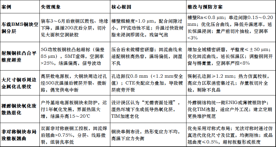
3.5 Typical Mass-Production Failure Cases and Corrective Actions
Based on field experience in automotive, communications, and industrial power sectors, common failure cases and targeted countermeasures are summarized:
IV. Conclusion
Embedded copper coin and pedestal thermal management technologies are essential for overcoming traditional PCB cooling bottlenecks and addressing localized high heat flux challenges. They significantly reduce junction temperatures of high-power components, suppress high-temperature aging and stress-related failures, and comprehensively enhance equipment reliability throughout its lifecycle. Among them, embedded copper coins offer high flatness and strong process compatibility, fitting standard SMT mass production flows while balancing performance and cost-effectiveness; raised copper pedestals minimize interfacial thermal resistance to achieve top-tier thermal efficiency, ideal for ultra-high-precision, ultra-low-resistance scenarios, albeit with higher process complexity and cost.
As equipment power density continues to rise, embedded copper structures are evolving toward larger sizes, greater complexity, and higher precision. Concurrently, reliability risks—including thermal stress mismatch, resin voids, drilling/plating defects, flatness deviations, PTH fatigue, SMT errors, and electrical insulation failures—are intensifying. These risks are often latent, cumulative, and batch-wide, making them difficult to detect through conventional inspection. A standardized, end-to-end control system spanning design, manufacturing, assembly, and validation is therefore essential.
In engineering practice, the principles of “front-loaded design, simulation-driven optimization, rigorous process control, and comprehensive validation” must be upheld. Multi-team collaborative planning should begin early in the project, with precise selection based on thermal load, iterative simulation-based optimization of structural parameters and layout, strict adherence to IPC standards, and thorough reliability testing—ultimately achieving an organic unity of thermal performance, manufacturability, and long-term reliability to ensure stable operation of high-end electronic equipment under harsh conditions such as thermal cycling, vibration/shock, and continuous duty.
trending news
Contact Us