



Sorry, no sales person is available right now to take your call. Pls leave a message and we will reply to you via email as soon as possible.
Home/ PCB News/ Core Support for Ceramic Substrate Reliability: Underlying Logic and Solution Breakdown of Ceramic PCB Plating Process
Core Support for Ceramic Substrate Reliability: Underlying Logic and Solution Breakdown of Ceramic PCB Plating Process
2026-08-12
Ceramic circuit boards are widely used in RF communication modules, high-power device packaging, high-end LED substrates, and automotive power electronics due to their excellent thermal conductivity, extremely low high-frequency loss, high insulation strength, and high-temperature resistance. As a critical step in the back-end manufacturing process of ceramic PCBs, plating directly affects the long-term stability of the substrate, soldering reliability of components, and product service life.
Exposed copper traces on ceramic substrates are highly susceptible to oxidation, corrosion, and sulfidation when left in air for extended periods, leading to failures such as open circuits, poor contact, signal attenuation, and soldering defects. The plating process forms a dense and uniform metallic protective layer over copper traces, effectively isolating them from air, moisture, dust, and corrosive agents to block degradation pathways. Simultaneously, it enhances pad flatness and solderability, improving yields in surface-mount assembly, wire bonding, and packaging processes. Thus, plating is essential for ensuring the high reliability of ceramic substrates. Different plating materials and processes vary significantly in performance, cost, and application suitability. This article systematically analyzes the two main plating process modules for ceramic PCBs and compares the characteristics and applications of mainstream surface plating solutions.
I. Two Main Plating Process Directions for Ceramic PCBs
Plating for ceramic circuit boards primarily consists of two complementary modules: via wall plating and surface metal coating treatment, which jointly ensure electrical interconnection and protective performance.
1. Via Plating – Establishing Interlayer Conductive Pathways
After laser drilling, the via walls of ceramic substrates undergo slight melting and crystalline changes due to thermal effects, resulting in an insulating and rough surface that cannot conduct electricity directly. Therefore, via plating is required to create a conductive path.
Standard process: A low-viscosity, specialized conductive ink is applied to the via walls and cured at high temperature to form a highly adherent conductive base. Pure copper is then electrodeposited uniformly onto the via walls, fully encapsulating the inner surfaces. This step establishes a low-impedance, stable conductive channel between the top and bottom copper layers, enabling interlayer transmission of current and signals—making it critical for 3D interconnection in multilayer ceramic PCBs. Pure copper is commonly used for via conductive layers due to its excellent conductivity, adhesion, and mechanical stability, meeting the demands of high-frequency and high-current applications.
2. Surface Coating Treatment – Protection and Solderability Enhancement
Surface coating treatment targets exposed copper pads, traces, and functional lines, depositing a dense metallic protective film via electrochemical or chemical displacement methods. Its core benefits include:
Long-term anti-corrosion and oxidation resistance: It completely isolates moisture, oxygen, and corrosive contaminants, preventing copper oxidation, corrosion, and discoloration, thereby enhancing storage stability and long-term operational reliability.
Optimized solderability: A smooth, uniform coating improves solder wettability and spreadability, avoiding defects such as cold solder joints, dewetting, and pad lifting, thus increasing yields in surface-mount assembly and wire bonding—especially crucial for precision miniaturized packaging.
II. Comparison of Mainstream Surface Plating Solutions by Performance and Application
Based on coating material, deposition mechanism, and process characteristics, six mature plating solutions have emerged in the industry, each with distinct advantages in protection, solderability, wear resistance, cost, and suitability for specific operating conditions, allowing flexible selection.
1. Copper Plating (Base Layer Thickening)
Deposition Principle: Includes electrolytic copper plating (electrodeposition with external power) and electroless copper plating (autocatalytic deposition from solution), suitable for via thickening and surface trace reinforcement.
Performance Characteristics: Extremely low electrical resistance, strong adhesion, controllable thickness, and high structural integrity.
Cost Level: Very low.
Key Advantages: Balances electrical and mechanical performance, suitable for irregular vias and fine-line features, with broad applicability.
Main Limitations: Offers no surface protection; bare copper oxidizes easily. Used only for base layer thickening and not suitable as a final surface finish.
Typical Applications: Via thickening in multilayer boards, reinforcement of high-power traces, and processing of substrates with complex geometries.
2. Immersion Tin (Chemical Displacement Tin)
Deposition Principle: Pure chemical displacement reaction without electrolysis, depositing a pure tin layer on copper surfaces.
Performance Characteristics: Smooth surface, excellent wettability, lead-free and RoHS-compliant, with good soldering stability.
Cost Level: Low.
Key Advantages: Simple process, high yield, outstanding cost-performance ratio, and RoHS compliance.
Main Limitations: Moderate wear and environmental resistance; unsuitable for long-term storage or harsh operating conditions.
Typical Applications: Consumer electronics ceramic substrates, standard LED carriers, and general-purpose power devices—ideal for mid-to-low-end products under mild operating conditions.
3. Electroless Nickel Immersion Gold (ENIG)
Deposition Principle: Electroless nickel barrier layer + immersion gold top layer, deposited without electrolysis, ensuring uniform coating.
Performance Characteristics: Excellent oxidation and corrosion resistance, long-lasting solderability, effective suppression of copper migration, and superior high-frequency signal stability.
Cost Level: High.
Key Advantages: Exceptional overall reliability, no degradation during long-term storage, and excellent soldering yield.
Main Limitations: High gold cost; not suitable for applications involving frequent mechanical abrasion.
Typical Applications: Precision RF components, high-end IC packaging substrates, military and medical-grade boards, high-frequency/high-speed devices, and high-reliability products requiring long-term storage.
4. Immersion Silver (Chemical Displacement Silver)
Deposition Principle: Silver ions in solution displace and deposit to form a thin, dense silver layer.
Performance Characteristics: Low impedance, excellent high-frequency conductivity, smooth surface, and short processing cycle.
Cost Level: Medium to low.
Key Advantages: Outstanding high-frequency performance, efficient processing, and good short-term oxidation resistance.
Main Limitations: Poor long-term environmental stability; prone to oxidation and tarnishing during extended storage.
Typical Applications: Mid-to-high-end consumer substrates with short delivery cycles and rapid assembly requirements, and standard high-frequency modules (to be packaged promptly after processing).
5. Electrolytic Hard Gold Plating (Thick, Wear-Resistant Gold)
Deposition Principle: Nickel underlayer as a diffusion barrier, followed by electrolytically thickened gold layer with controlled hardness and density.
Performance Characteristics: High hardness, excellent wear and insertion/extraction resistance, and strong mechanical stability.
Cost Level: Very high.
Key Advantages: Withstands repeated press-fit, bonding, and mating cycles while maintaining both conductivity and mechanical protection.
Main Limitations: Complex process and high cost; low cost-effectiveness for standard consumer applications.
Typical Applications: Automotive high-power electronics, industrial control systems, aerospace components—ideal for harsh environments requiring frequent mechanical contact.
6. General Electrolytic Plating (Multi-Metal Customization)
Deposition Principle: The substrate acts as the cathode, with the target metal as the anode; directional deposition occurs under electrical current, compatible with various metals (nickel, tin, gold, etc.).
Performance Characteristics: Precise thickness control, excellent uniformity, suitable for complex geometries and thick coatings.
Cost Level: Medium.
Key Advantages: Highly versatile; supports both via thickening and surface coating, meeting customized requirements.
Main Limitations: Requires electrical current; more complex than chemical methods, with lower efficiency for thin coatings.
Typical Applications: High-precision custom substrates, thick or irregularly shaped coatings, and non-standard products with special electrical or protective requirements.
III. Process Summary and Selection Logic
Plating is a core process determining the electrical performance, protective capability, and service life of ceramic substrates. Via plating ensures interlayer connectivity, while surface coatings provide protection and solderability. Practical selection should consider operating conditions, environmental severity, soldering/bonding requirements, signal frequency, and cost budget:
General consumer applications, cost-sensitive: Use copper plating (base) + immersion tin.
Short delivery cycles, rapid mass production: Immersion silver offers good cost-performance balance.
Precision high-frequency, long-term reliability: ENIG is the preferred choice.
Frequent friction, repeated mechanical operations: Electrolytic hard gold is optimal.
Custom non-standard, special coating requirements: General electrolytic plating enables flexible processing.
Accurate matching of plating solutions maximizes the overall performance and service life of ceramic circuit boards.
IV. Summary Comparison Table of Key Parameters and Application Scenarios
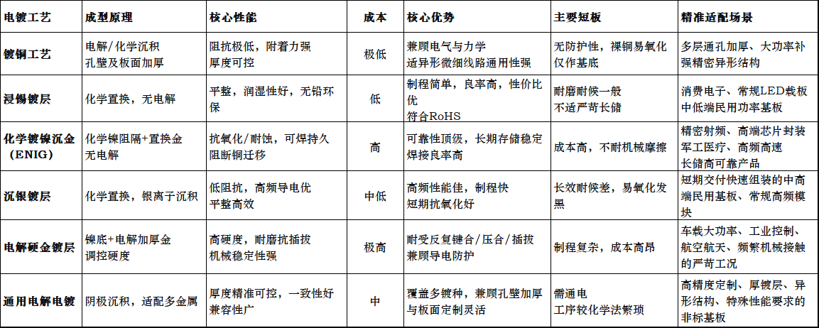
Quick Selection Guide: Basic cost control → Copper + Immersion Tin; Short-term mass production → Immersion Silver; High reliability & long storage → ENIG; Harsh friction → Electrolytic Hard Gold; Custom non-standard → General Electrolytic Plating. Rational selection is key to unlocking the ultimate performance and longevity of ceramic substrates.
trending news
Contact Us