



Sorry, no sales person is available right now to take your call. Pls leave a message and we will reply to you via email as soon as possible.
Home/ PCB News/ 10-Layer 1~4 Step and AnyLayer HDI Stackup Structure and Impedance Design Specification
10-Layer 1~4 Step and AnyLayer HDI Stackup Structure and Impedance Design Specification
2026-08-07
Ten-layer HDI is categorized into five types based on microvia stacking structures: 1-step, 2-step, 3-step, 4-step, and Anylayer (ELIC – Every Layer Interconnect). A higher step count indicates more stacked blind vias and greater routing density, meeting the demands of miniaturized, high-compute end devices. Currently, 3-step, 4-step, and Anylayer ten-layer HDI are mainstream in consumer electronics, servers, and AI computing motherboards.
1-Step HDI: Features only single blind vias between the outer layer and the adjacent inner layer, with no stacked vias. It has the simplest process and lowest cost, suitable for mid-to-low-end smart devices;
2-Step HDI: Uses two laser-drilled blind via steps, supporting stacked or staggered vias, offering improved routing density—commonly used in mid-range smartphones and industrial control motherboards;
3-Step / 4-Step HDI: Employs multi-layer stacked blind vias with fine lines and small holes, enabling high-density routing—the standard for flagship smartphones, tablets, and automotive computing boards;
Anylayer (ELIC – Any Layer): Every Layer Interconnect allows laser-drilled blind vias between any two layers, eliminating traditional core board limitations. It enables extreme thinness and miniaturization, serving as the core substrate for premium foldable displays and advanced AI modules.
Process Standard Note: BAINENG Cloud Board’s ten-layer HDI shares identical lamination, laser drilling, and impedance control processes with its eight-layer full-step HDI system. Stack-up design rules, impedance calculation baselines, and material selection standards can directly refer to the technical document “Eight-Layer HDI (1-Step, 2-Step, 3-Step, Any Layer) Stack-up and Impedance.”
Document.
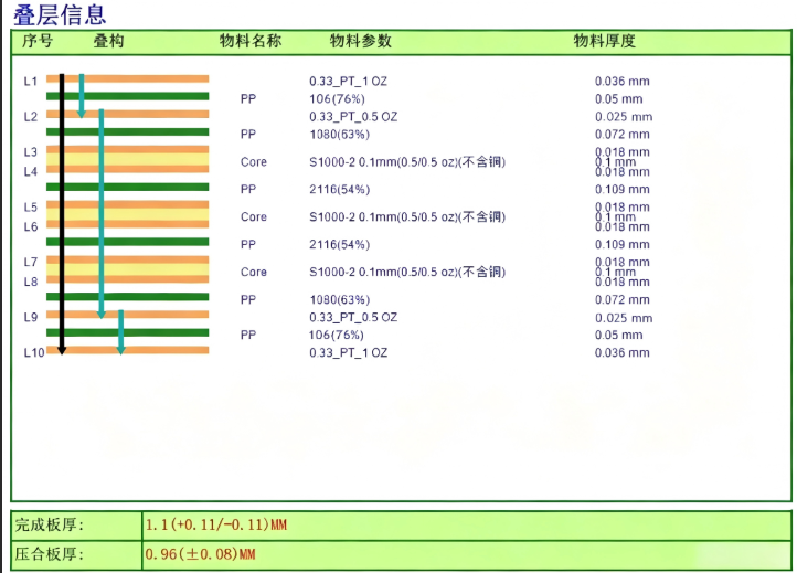
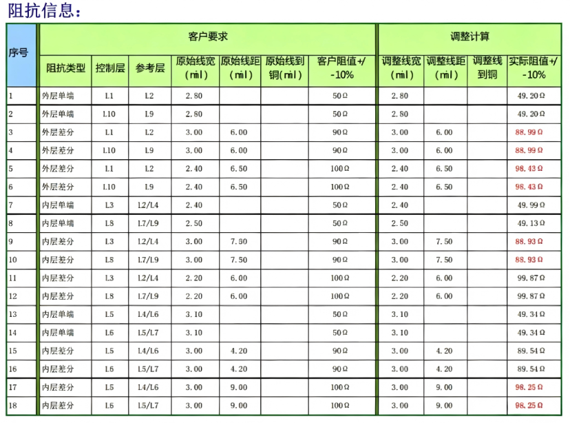
Based on the stack-up and process characteristics of the aforementioned ten-layer HDI variants, 10-layer and 12-layer Anylayer (Any Layer) HDI have become the dominant specifications for high-end consumer devices. Compared to conventional 1–4-step HDI, Anylayer’s arbitrary interconnect technology offers ultra-high routing density, extreme thinness, and flexible interlayer connectivity—making it widely adopted in premium smartphones, wearables, and AI-enabled precision electronics.
Apple was the world’s first smartphone brand to mass-produce motherboards using Anylayer HDI. Starting with the iPhone 4S, which featured a 10-layer, 5-step Anylayer HDI motherboard (using five laser drilling steps), this advanced HDI technology rapidly gained industry adoption. Domestic leaders like Huawei, OPPO, and Xiaomi soon followed, integrating Anylayer HDI into their flagship models to significantly enhance device integration and performance.
Tracing Apple’s motherboard evolution reveals four key phases that have guided the PCB industry’s technological advancement: Phase 1 used conventional multilayer PCBs—mature but low-density; Phase 2 adopted 1–3-step standard HDI boards (typically 8–12 layers), greatly improving integration; Phase 3 began with the iPhone 4S as a milestone, introducing 5-step, 10-layer Anylayer HDI to overcome traditional step-based routing limitations; Phase 4 marked a turning point with the iPhone X, which pioneered SLP (Substrate-Like PCB) technology, and since 2020, Apple has fully transitioned its entire lineup to SLP, completing the shift from high-end HDI to substrate-like boards.
In terms of manufacturing and cost, HDI motherboard complexity and expense scale directly with blind via step count, following a clear upward trend. Each additional HDI step imposes stricter requirements on laser drilling, lamination planarization, and impedance control, increasing process complexity, fabrication difficulty, and overall manufacturing cost. Ten-layer Anylayer HDI breaks through the interlayer connectivity constraints of traditional 1–4-step HDI, requiring multiple precise laser drills and full-layer, high-fidelity impedance simulation and control—thus commanding significantly higher process costs and belonging to the realm of premium, precision PCB manufacturing.
The following image shows BAINENG Cloud Board’s standard ten-layer, 2-step HDI stack-up structure:
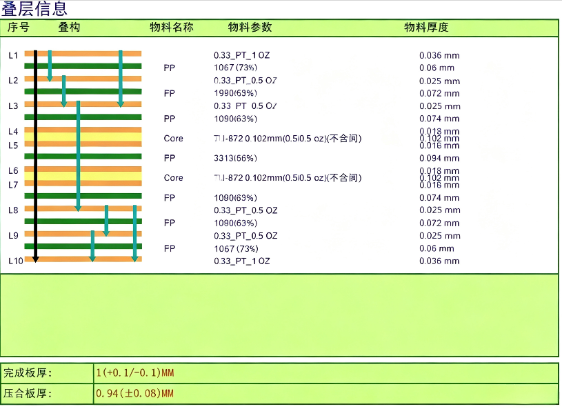
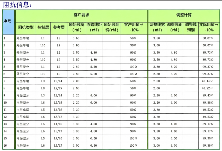
Currently, mainstream high-end HDI boards use subtractive processes to manufacture ELIC (Every Layer Interconnect) Anylayer substrates. As terminal device integration continues to advance, high-end Anylayer HDI demands finer line/space capabilities—shrinking from 50μm down to the 30μm range. Traditional subtractive plating for any-layer HDI can no longer meet these ultra-fine line requirements, necessitating a shift to semi-additive processes for mass production. Semi-additive processing, long established in IC substrate manufacturing, produces HDI boards with performance approaching substrate standards—industry-wide referred to as SLP (Substrate-Like PCB).
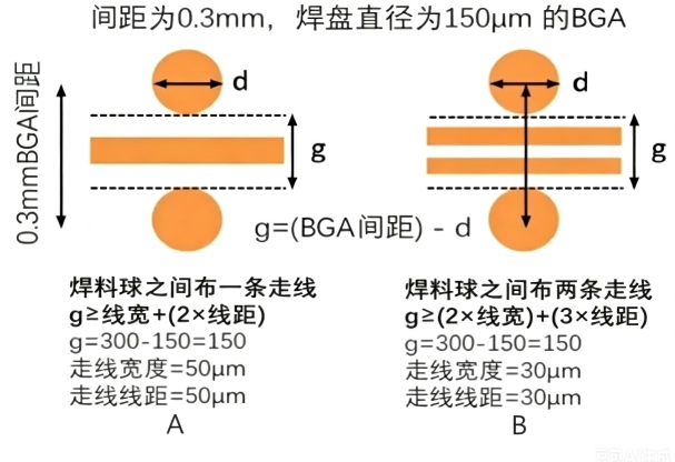
The following image shows BAINENG Cloud Board’s standard ten-layer, 3-step HDI stack-up structure:
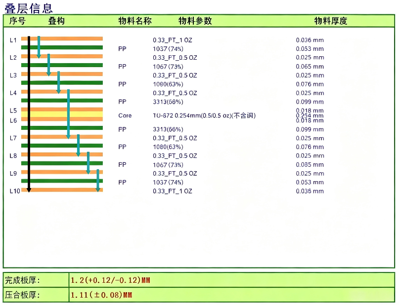
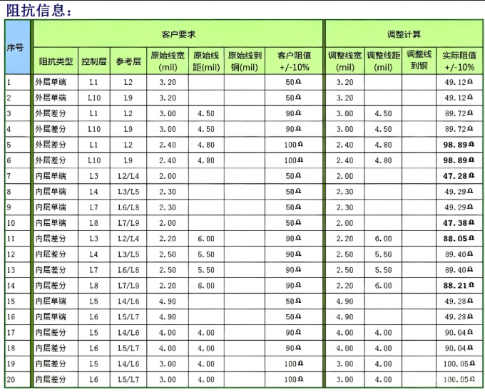
The following image shows BAINENG Cloud Board’s standard ten-layer, 4-step HDI stack-up structure:
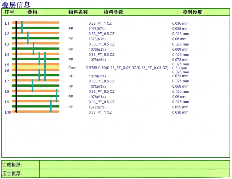
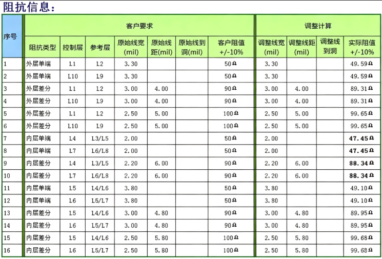
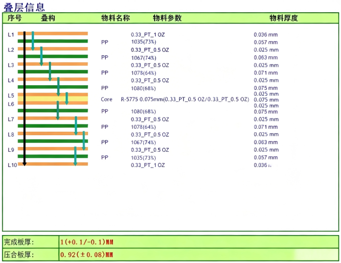
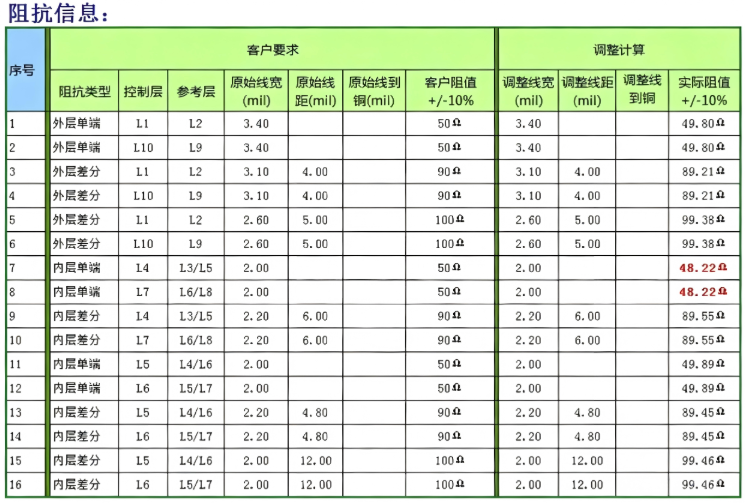
The following images show BAINENG Cloud Board’s standard ten-layer Any Layer (Any Step) HDI stack-up structure and impedance details:
trending news
Contact Us