



Sorry, no sales person is available right now to take your call. Pls leave a message and we will reply to you via email as soon as possible.
Home/ PCB News/ ABF Substrate, BT Substrate, and Glass Core: Understanding the Fundamental Differences
ABF Substrate, BT Substrate, and Glass Core: Understanding the Fundamental Differences
2026-09-28
As AI computing chips evolve towards larger dimensions and multi-chiplet heterogeneous integration, the package substrate, as the core base of the chip, directly determines high-density interconnect capability, signal integrity, and packaging yield. BT substrates, ABF substrates, and glass-core substrates represent mature organic substrate solutions, current mainstream high-end computing solutions, and potential next-generation upgrade directions, respectively. These three are not simple iterative replacements but form a tiered application landscape based on cost, performance, and process maturity.
I. BT Substrates: Mature and Reliable, but with Performance Ceilings
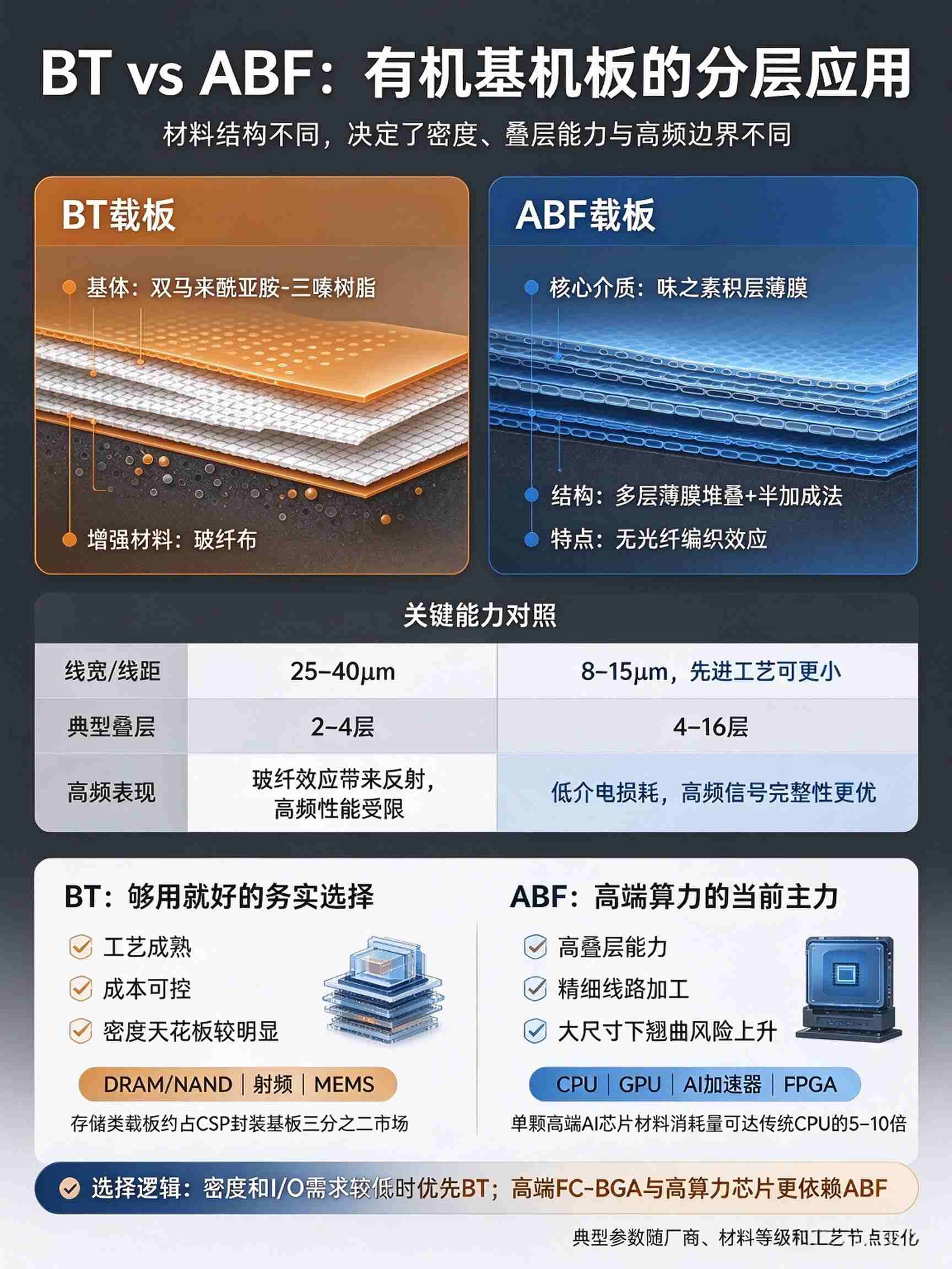
BT substrates use bismaleimide triazine (BT) resin as the matrix, impregnated with glass fiber cloth and laminated into a single piece. They feature high hardness, excellent dimensional stability, and good heat resistance, making them the most mature organic packaging substrate solution currently available.
However, its technical limitations are equally prominent: BT resin is relatively rigid, making drilling difficult and limiting micro-via processing capabilities. Line width/line spacing typically remains in the range of 25~40μm, and layer counts are concentrated at 2~4 layers, making it difficult to break through wiring density limits. This characteristic dictates that BT substrates cannot support high-density interconnect requirements involving tens of thousands of pins.
Therefore, the main applications of BT substrates are concentrated in scenarios such as memory chips (DRAM, NAND), RF modules, and MEMS sensors—fields that demand high reliability but do not strictly require high wiring density. Memory-class substrates account for approximately two-thirds of the market share in the CSP packaging substrate domain, representing the most important downstream market for BT substrates.
In short, BT substrates are a pragmatic choice of "good enough": costs are controllable and processes are mature, but there is a clear ceiling.
II. ABF Substrates: Core Carriers for High-Density Interconnects, Approaching Physical Limits
The core material of ABF substrates is Ajinomoto Build-up Film, which contains no glass fiber cloth. It is manufactured using multi-layer film stacking combined with semi-additive processes, enabling mass production line widths/spacings of 8~15μm, with advanced processes allowing for further miniaturization.
Core Advantages:
Low Dielectric Loss: The absence of a glass fiber structure avoids signal reflection caused by fiber weave effects, resulting in significantly better high-frequency signal integrity compared to BT substrates;
High Layer Count Capability: Supports stacking of 4~16 layers or even more, adapting to FC-BGA packaging needs for high I/O density chips such as CPUs, GPUs, AI accelerators, and FPGAs;
High Surface Flatness: Consistent via filling and wiring quality makes it suitable for fine-line processing.
Inherent Shortcomings:
The physical bottleneck of ABF substrates lies in thermal expansion mismatch. The planar coefficient of thermal expansion (CTE) of conventional ABF materials is approximately 13~17 ppm/℃, while the Z-axis CTE reaches as high as 48 ppm/℃. In contrast, the CTE of silicon chips is only about 2.6 ppm/℃, creating a five-fold difference. As chip packaging areas continue to expand, this mismatch causes severe warping of organic materials during lamination and thermal cycling. The larger the substrate area, the harder it becomes to control warping, directly impacting lithography and placement accuracy. Additionally, the measured dielectric loss of ABF at high frequencies can exceed 0.018 in the 10GHz range, making signal attenuation issues increasingly prominent in high-frequency scenarios.
Regarding material supply, Ajinomoto holds over 95% of the global market share for ABF materials used in GPU and CPU packaging substrates, indicating extremely high supply concentration. As AI chip sizes increase and layer counts rise, the amount of ABF material consumed per high-end AI chip reaches 5 to 10 times that of traditional CPUs, leading to persistently tight supply-demand relations.
III. Glass Substrates: Material Upgrade Born for Next-Generation Computing
First, a common misconception must be clarified: Glass substrates do not "replace ABF substrates" . The technical route for glass substrates involves replacing the traditional organic core board with a glass core (rather than replacing the ABF film itself). ABF remains as an insulating build-up material on both sides of the glass core. Chip interconnection functions are realized jointly by the chip-side RDL, glass vias/copper interconnect structures, and ABF build-up layers. Glass and ABF coexist in a complementary relationship.
Core Advantages:
Thermal Expansion Matching: The CTE of glass is approximately 3.2 ppm/℃, highly matching that of silicon chips, which fundamentally suppresses warping and solder joint fatigue caused by thermal cycling;
Ultra-Flat Surface: Surface roughness is less than 0.1μm, ensuring high-precision etching of fine lines and supporting line widths/spacings below 2μm;
Low Dielectric Loss: As an insulator, glass has a loss factor approximately 10 times lower than traditional organic substrates, supporting high-speed signal transmission exceeding 112Gbps;
High Stiffness: Young's modulus ranges from 50~90GPa, several times that of organic materials, making large-size substrates resistant to deformation.
Industrialization Challenges:
Mass production of glass substrates faces multiple process challenges. TGV (Through-Glass Via) processing yield is the core bottleneck, with issues such as hole precision, defect-free copper filling, copper adhesion, multi-layer RDL alignment, and thermal cycle reliability not yet fully resolved. Current full-process mass production yield is around 50%~60%, requiring improvement to above 75%. Furthermore, manufacturing and cutting of large-size ultra-thin glass, panel-level alignment, and mass production cost control are key hurdles in moving from laboratory to scalable commercial application.
Mainstream technology routes fall into two categories:
One is as a glass-core substrate, replacing the organic core board with glass and pairing it with ABF build-up for BGA/CSP/2.5D packaging; the other is as a glass interposer, replacing silicon interposers with glass for CoWoS and other 2.5D/3D packaging scenarios, using square glass panels to achieve larger packaging areas and lower costs.
IV. Essential Differences Among the Three
If the chip is likened to a house, the substrate is the foundation—BT is a solid old-style concrete foundation, ABF is a precise reinforced concrete structure, and glass substrates are a new composite material foundation combining high strength with thermal matching.
The table below intuitively presents the core differences among the three across eight dimensions:
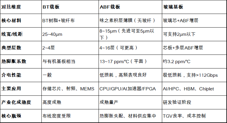
The relationship among the three is not simple iterative replacement. BT substrates retain advantages in cost and maturity for mid-to-low-end scenarios; ABF substrates are the primary packaging substrate for current high-end computing chips, but their physical limits are being constantly approached; glass substrates represent the material upgrade direction for meeting the demands of next-generation larger and denser packaging, though industrialization still requires time. Understanding the boundaries and applicable scenarios of all three is far more valuable than debating who will "replace" whom.
trending news
Contact Us