



Sorry, no sales person is available right now to take your call. Pls leave a message and we will reply to you via email as soon as possible.
Home/ PCB News/ PCB Material Characteristics and In-Depth Analysis of High-Speed Signal Integrity
PCB Material Characteristics and In-Depth Analysis of High-Speed Signal Integrity
2026-09-29
For electronic hardware engineers, PCB layout engineers, and SI (Signal Integrity) engineers, PCB material and stack-up design are the core foundational elements of high-speed circuit design. The vast majority of engineering issues—such as excessive return loss on high-speed links, insertion loss exceeding budget, poor impedance consistency, board-level delamination, and via reliability failures—are fundamentally rooted in misconceptions regarding PCB material parameters, process characteristics, and signal transmission mechanisms.
In hardware board systems, the PCB is not merely a basic carrier for mounting components. Core metrics such as the dielectric parameters of the substrate, copper foil thickness and surface roughness, lamination dielectric thickness precision, and reference plane continuity directly determine the transmission and return characteristics of high-speed signals and affect overall system thermal dissipation capabilities. This article systematically deconstructs PCB material selection logic, thermal reliability parameters, copper foil characteristics, and dielectric loss mechanisms, linking fundamental material properties to board-level engineering problems to provide standardized technical basis for high-speed PCB design, material selection, project reviews, and issue resolution.
This is Part 1 of a series, focusing on PCB material composition and selection logic, the core meaning of PCB thermal reliability (Tg), the engineering impact of copper thickness and copper foil roughness, and the correlation between dielectric loss and high-speed signal integrity. Part 2 will focus on stack-up design specifications, interpretation of impedance control sheets, methods for identifying fab house stack-up tables, solutions for common engineering issues, and project review standards.
Note: Material parameters mentioned herein are mostly industry typical values or published parameters for specific models. Actual designs should rely on the latest datasheets from material suppliers, post-lamination measured data from fab houses, and corresponding test standards.
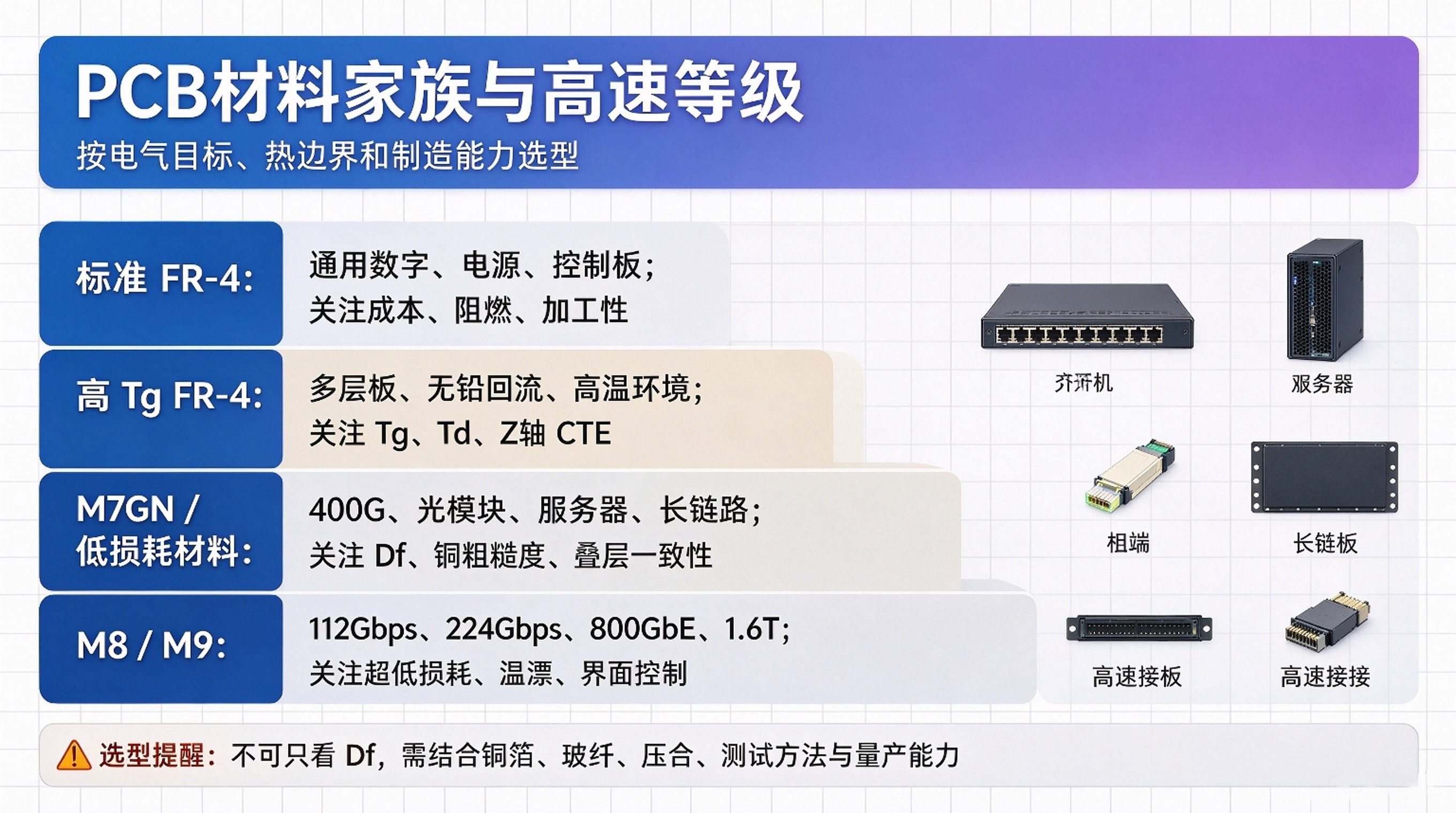
I. Composition of PCB Materials and Engineering Selection Logic
The core substrate system of a PCB consists of three main components: copper foil, epoxy resin, and glass fiber cloth. The industry-standard copper-clad laminate (core) is a pre-cured integrated structure with stable performance and high thickness precision; prepreg (PP) is an incompletely cured resin-glass composite that flows under heat during lamination to fill inter-layer gaps, bonding adjacent copper layers together upon cooling and curing.
The electrical, thermal, mechanical reliability, and processing characteristics of the finished PCB are jointly determined by the core type, PP part number, copper foil specification, plating process, and lamination process. The theoretical dielectric thickness noted at the design stage is only a reference value; final actual parameters must be based on post-lamination measured data from the fab house, which is the core prerequisite for high-speed impedance design and SI simulation.
1. Non-Fixed Characteristics of PCB Dielectrics
It must be clarified in engineering practice: A PCB is not a uniform fixed dielectric; there is dynamic variation in the dielectric environment across the entire board. A single PCB may use combinations of multiple cores and PPs; even the same PP material can result in deviations in final cured thickness due to differences in resin content, copper foil pattern coverage on the board surface, and lamination pressure and temperature parameters.
Additionally, details such as the warp/weft weaving direction of the glass fiber cloth, the uniformity of resin filling between copper layers, local copper density, and solder mask thickness all alter the effective dielectric environment for signal transmission. Therefore, PCB material selection cannot rely solely on nominal Dk (dielectric constant) values. It requires comprehensive verification of material grade, glass fiber cloth model, resin content, target dielectric thickness, test frequency, and test standards to ensure parameters match high-speed design requirements.
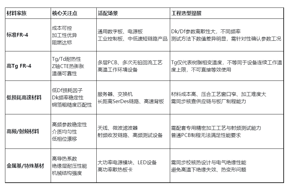
2. Engineering Positioning of Mainstream PCB Material Families
Different PCB material systems vary significantly in electrical performance, thermal reliability, manufacturing difficulty, and cost. Selection must be based on product scenarios, electrical metrics, thermal boundary conditions, mechanical environments, and mass production capabilities, avoiding the blind principle of "best parameter." The specific engineering applications, key considerations, and selection taboos for each material family are shown in the table below:
3. Correspondence Between Material Parameters and Engineering Risks
To avoid design oversights, engineering reviews can categorize PCB material parameters into four dimensions: electrical characteristics, thermal reliability, mechanical characteristics, and manufacturing characteristics. Each dimension corresponds to clear design constraints and verification standards, achieving controllable parameters and traceable risks:
Electrical Parameters: Dk determines signal transmission speed and impedance accuracy; Df dominates dielectric loss, directly affecting insertion loss, return loss, and eye diagram quality of high-speed links;
Thermal Parameters: Tg, Td, T260/T288, and Z-axis CTE characterize the substrate's resistance to thermal shock, delamination, and thermal expansion, determining board-level thermal cycling and reflow reliability;
Mechanical Parameters: Copper foil type, surface roughness, and substrate rigidity affect trace etching precision, hole wall reliability, and long-term structural stability;
Manufacturing Parameters: Resin content, lamination window, and process compatibility determine mass production consistency, preventing out-of-spec impedance and loss variations between batches.
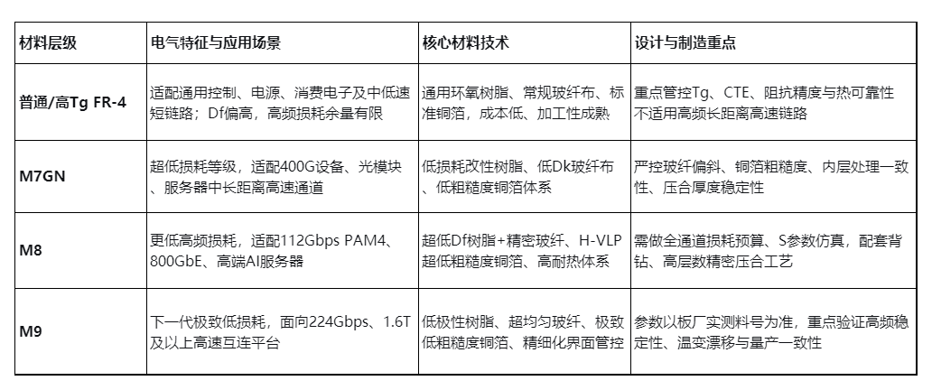
II. Performance Differences and Scenario Adaptation of FR-4, M7GN, M8, and M9 Substrates
In engineering, the performance boundaries between standard FR-4 and high-speed M-series substrates are often confused. M7GN, M8, and M9 are not IPC standard material grades but common industry terms for generations of Panasonic MEGTRON high-speed substrates. The electrical performance, process requirements, and supported data rates differ greatly among these levels, requiring precise matching to project needs.
1. FR-4 is a Material System, Not a Single Grade
FR-4 is a general term for glass-reinforced epoxy laminate substrates meeting the UL94 V0 flame retardant standard, not a single material with fixed parameters. Standard FR-4, medium-high Tg FR-4, and low-loss FR-4 show obvious differences in Tg temperature, Dk/Df parameters, moisture absorption, thermal decomposition temperature, Z-axis thermal expansion coefficient, and process windows.
Marking only "FR-4" in drawings or BOMs typically meets the design requirements for low-speed control boards and power supplies but cannot adapt to high-frequency high-speed scenarios such as high-speed switches, AI servers, and long-distance SerDes links, easily leading to issues like excessive loss and timing deviation.
Definition of Industry-Mainstream M-Series High-Speed Substrates: M7GN refers to the low-Dk glass version R-5785(GN) of the Panasonic MEGTRON 7 series; M8 corresponds to ultra-low loss materials at the same level as MEGTRON 8; M9 is the next-generation high-end high-speed substrate targeting speeds of 224Gbps and above. In project designs, do not vaguely label M7/M8/M9; you must specify the supplier, laminate/PP part numbers, glass fiber cloth specifications, copper foil types, and test standards.
2. M7GN: Mature Mass-Produced Ultra-Low Loss High-Speed Substrate
M7GN is an optimized version of the MEGTRON 7 material system paired with dedicated low-Dk glass fiber cloth. Its core advantage lies not just in reducing Df loss but also in precisely controlling Dk parameter uniformity, glass weave effect, and differential link delay skew, offering high cost-performance among mature mass-produced high-speed substrates.
According to official parameters, R-5785(GN) has a typical Df value of 0.0021~0.0023 at the 14GHz band, with slight fluctuations depending on core structure and resin content. This material is widely used in 400G optical modules, high-speed switches, routers, server motherboards, and long-distance PCIe and Ethernet SerDes links.
Engineering Focus: The performance gains of M7GN require supporting processes. It must be paired with low-roughness copper foil, standardized inner layer brown oxide treatment, stable lamination thickness control, and S-parameter verification. If only the resin material is upgraded while retaining high-roughness copper foil and standard processes, the optimization effect on high-speed loss will be significantly diminished.
3. M8: Lower Loss Substrate for 112Gbps PAM4 and 800GbE
MEGTRON 8 substrates further reduce high-frequency transmission losses by optimizing resin polarity, glass structure, and copper foil compatibility. For mainstream models like Panasonic R-5795(U)/R-5795(N), Dk is 3.08~3.13 and Df is 0.0012~0.0016 at 14GHz, with DMA Tg reaching up to 220°C; transmission loss at the 28GHz band is approximately 30% better than M7GN, with significantly improved heat resistance and high-frequency stability.
This substrate primarily adapts to 112Gbps PAM4 long-distance channels in 800GbE switches, AI servers, high-end optical transmission equipment, and base station equipment. Upgrading to this material level is no longer a simple component replacement; it requires synchronizing low-Df glass fiber, ultra-low roughness copper foil, refined inner layer processing, back-drilling processes, and high-layer-count precision lamination technology, placing extremely high demands on fab house process capabilities.
4. M9: Next-Generation High-Speed Substrate for 224Gbps
M9 is a high-end substrate developed for 224Gbps SerDes, 1.6T switching systems, and next-generation AI server interconnect scenarios. Its core goal is to minimize high-frequency loss while strictly controlling Dk/Df drift, phase deviation, and delay fluctuation under varying temperature conditions.
Currently, the MEGTRON 9 technical solution has completed verification, but its mass production maturity is lower than M7 and M8. In engineering design, do not directly apply generic parameters for simulation; you must request datasheets, test methods, copper/glass combination schemes, and mass production qualifications for the specific version from the fab house.
Key Characteristics: The systemic bottleneck for M9 substrates is no longer limited to single resin loss. The impact of manufacturing details such as copper foil roughness, glass dielectric uniformity, lamination thickness variation, and via parasitic discontinuity increases significantly. Minor process deviations can cause high-speed link failures, requiring a joint modeling and verification development mode involving material manufacturers, fab houses, connector vendors, and SI teams.
5. Panoramic Comparison of Standard and High-Speed Substrates
6. Core Principles of Substrate Selection and Mixed Lamination Design Schemes
Substrate upgrades do not need to blindly cover the entire board. The core basis includes signal rate, rise time, trace length, number of connectors, via structures, bit error rate requirements, and operating temperature. For the same interface (e.g., PCIe, Ethernet), short-distance direct links can use low-loss FR-4, while long backplanes, multiple connectors, and high-temperature conditions require upgrading to M7GN/M8 substrates.
The economically optimal scheme is mixed lamination design: using low-loss high-speed substrates for high-speed signal layers and standard FR-4 substrates for power and low-speed control layers, balancing performance and cost. Mixed lamination designs require prior verification of resin compatibility, lamination process windows, and Z-axis CTE matching to avoid board warpage and inter-layer delamination issues.
7. Core Technical Differences Between Standard and High-Speed Substrates
Resin System Differences: Standard FR-4 uses a generic epoxy system; high-speed substrates significantly reduce high-frequency dipole loss by lowering resin molecular polarity, optimizing cross-linking structures, and introducing PPE/PPO modified systems.
Glass Cloth Differences: High-speed substrates focus not only on cloth style but also strictly control the intrinsic Dk of the glass, warp/weft weaving uniformity, and spread glass effects, eliminating local dielectric non-uniformity.
Copper Foil and Interface Differences: Using VLP/H-VLP/RTF low-roughness copper foils reduces high-frequency skin effect losses while precisely balancing copper smoothness and resin adhesion.
Parameter Stability Differences: High-speed substrates prioritize managing the variation of Dk/Df with frequency, temperature, and batch, rather than relying on nominal parameters at a single frequency point, ensuring stability across all operating conditions.
Manufacturing Control Differences: Stricter requirements for dielectric thickness, etched trace profile, copper surface uniformity, and impedance coupon consistency, resulting in lower process tolerance.
Verification System Differences: Standard substrates only require routine electrical tests; high-speed substrates require a complete verification loop established through TDR, VNA, insertion/return loss, differential skew, eye diagrams, and bit error rate testing.
8. Engineering Interpretation of Key Thermal Parameters (Tg/Td/CTE)
Tg (Glass Transition Temperature): Refers to the critical temperature at which the resin transitions from a hard glassy state to a flexible rubbery state. Values differ depending on the test method (DMA/TMA). As temperature approaches Tg, substrate modulus, dimensional stability, and dielectric properties degrade significantly. Standard FR-4 Tg is approx. 130~170°C, high-Tg FR-4 is approx. 170~200°C, and M8 high-speed substrates can reach 220°C. Core Taboo: Tg is a process tolerance temperature and cannot be equated to the maximum continuous operating temperature of the device. Long-term operating temperature must be assessed comprehensively considering heat dissipation, hotspots, and copper losses.
Td (Decomposition Temperature), T260/T288 Heat Resistance Duration: Td characterizes the critical temperature for high-temperature decomposition of the resin; T260/T288 represents the duration the substrate resists delamination and failure at fixed high temperatures, directly determining the reliability of lead-free reflow and thermal cycling tests.
Z-Axis CTE (Coefficient of Thermal Expansion): Characterizes thermal expansion properties in the board thickness direction. In multi-layer boards, heavy copper boards, and high aspect ratio through-hole scenarios, the difference in thermal expansion between resin and copper accumulates thermal stress, easily causing hole wall cracking and inter-layer delamination after repeated thermal cycling. It is a core metric for high-speed multi-layer board reliability reviews.
Lead-Free Reflow Process Adaptation: Lead-free processes have higher peak temperatures and more thermal shock cycles. Standard FR-4 is prone to delamination and via damage. High-Tg and M7GN/M8 substrates improve thermal stability, but must be matched with reasonable lamination parameters, copper pattern density, and reflow profiles to achieve closed-loop process reliability.
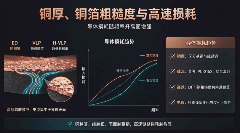
III. Copper Thickness, Copper Foil Roughness, Current Carrying Capacity, and High-Speed Loss Characteristics
1. Precise Definition of Engineering Copper Thickness
Industry standard nominal copper thickness: 0.5oz≈17.5μm, 1oz≈35μm, 2oz≈70μm. These values represent the nominal thickness of the base material, not the actual finished thickness. Inner layer copper thickness is reduced by the etching process, while outer layer copper thickness is increased by pattern plating.
In engineering design, one must distinguish between base copper thickness, post-process copper thickness, and post-plating finished copper thickness. Impedance calculations, current carrying simulations, and annular ring strength designs must uniformly use measured finished copper thickness to avoid design deviations caused by parameter confusion.
2. Bidirectional Impact of Copper Thickness on Electrical, Thermal, and Process Capabilities
Copper foil thickness is strongly correlated with board performance and process capability: Heavy copper reduces DC resistance, lowers voltage drop, and improves heat dissipation and current carrying capacity, suitable for high-power supply scenarios; however, greater copper thickness increases the difficulty of fine line etching, high-density BGA routing, and precise impedance control, making issues like width deviation, shorts, and solder mask anomalies more likely.
High-current carrying designs must be precisely verified based on the IPC-2152 standard, considering actual board thickness, copper coverage, heat dissipation conditions, and allowable temperature rise. Do not directly apply generic formulas.
3. Mechanism of High-Speed Loss Due to Copper Foil Roughness
At low frequencies, copper foil roughness has no significant impact on signal transmission; however, in high-speed high-frequency scenarios, signal currents concentrate on the conductor surface (skin effect). Rough copper surfaces lengthen the current transmission path, significantly increasing conductor loss, leading to excessive link insertion loss and eye diagram closure.
For high-speed links of 25Gbps and above, both substrate Df and copper foil roughness must be included in the overall loss budget, prioritizing H-VLP and VLP series ultra-low roughness copper foils. Note that Rz and Rq roughness test standards vary by manufacturer, so parameters cannot be directly compared horizontally; fab house measured S-parameters should be the reference.
4. Impact of Plating and Vias on Copper Thickness Reliability
Outer layer pattern plating alters trace sidewall and surface copper thickness, causing width deviation and impedance drift; via plating thickness directly determines hole wall reliability under high-temperature thermal cycling and repeated reflows; pad surface finish affects solder joint contact stability.
In engineering reviews, high-speed links require focused checks on plating-induced width shifts, solder mask parasitics, and via discontinuities; high-current scenarios require verification of the overall DC impedance of traces, via arrays, and copper planes, not just referencing nominal copper thickness in the stack-up table.
IV. Core Mechanisms of Dielectric Loss and High-Speed Signal Integrity
1. Dk/Df and Effective Dielectric Environment
Dk (Dielectric Constant) determines signal transmission speed and characteristic impedance. Higher Dk results in greater signal propagation delay, and parameter fluctuations directly cause impedance and phase uncertainty. Df (Loss Tangent) is the core metric for dielectric loss. Larger Df leads to more severe signal attenuation, narrower high-speed eye diagrams, and smaller link budget margins.
Engineering Key: The nominal Dk/Df in substrate datasheets are parameters for pure resin or standard coupons. The effective dielectric constant of a finished PCB is the result of the combined action of resin, glass fiber, copper surface structure, routing geometry, and solder mask.
General Parameter Magnitude Reference: At the 1GHz band, standard FR-4 has Dk=3.8~4.5 and Df=0.012~0.020; low-loss high-speed materials can reduce Df to 0.002~0.008. Parameters measured under different test standards (IPC-TM-650, cavity resonator, stripline) cannot be directly compared across manufacturers. Simulations must use measured parameters matching the actual conditions.
2. Multi-Dimensional Composition of High-Speed Insertion Loss
Total insertion loss in high-speed links is not determined solely by dielectric Df but is the superposition of dielectric loss + conductor roughness loss + plating/process loss + via/connector discontinuity loss + radiation loss + termination mismatch loss.
In actual engineering, for high-frequency long-link scenarios, losses from copper foil roughness, via parasitics, and routing discontinuities often exceed dielectric losses. Therefore, optimizing high-speed signal integrity requires first establishing a full-link loss budget, then specifically optimizing materials, copper foil, traces, and via structures, rather than simply upgrading to high-end substrates.
3. Engineering Impact of Glass Weave Effect
The large difference in dielectric parameters between glass fiber (Dk≈6) and epoxy resin (Dk≈3), combined with the periodic non-uniformity of the glass weave, causes fluctuations in the local dielectric environment. If high-speed fine traces run parallel to glass bundles or cross glass regions for extended periods, issues such as local impedance shift, intra-pair differential timing skew, and excessive phase error arise.
In high-speed differential link design, optimize trace angles, width/spacing, and reference plane distance based on glass cloth style and weave structure. For ultra-high precision scenarios, consider using spread glass cloth and high-resin content systems to minimize parameter fluctuations caused by the weave effect.
4. Stability Management Across Frequency, Temperature, and Batch
Dk/Df parameters exhibit obvious frequency dispersion and temperature dependence: as frequency increases, dielectric loss grows non-linearly; under high/low temperature conditions, parameter drift leads to eye diagram degradation and timing offset. Additionally, variations in resin content and process fluctuations cause inter-batch parameter differences, leading to mass production consistency issues.
High-speed projects require full-process parameter traceability: simulation parameters, impedance control sheets, fab house stack-up parameters, and measured S-parameters must correspond one-to-one. Real-board verification is completed via TDR, VNA, eye diagram, and bit error rate testing, matching product speed and risk levels.
V. Summary of PCB Material Impact on High-Speed Signal Integrity
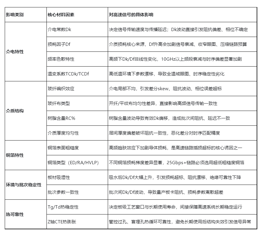
In summary, PCB material selection is not a simple comparison of Dk/Df values but a systematic trade-off involving electrical performance, thermal reliability, mechanical structure, process capability, mass production consistency, and cost/supply chain. Only by jointly considering material parameters, fab house processes, and actual high-speed link conditions can we fundamentally reduce high-speed signal integrity risks.
Part 2 will focus on stack-up design specifications, interpretation of impedance control sheets, methods for identifying fab house stack-up tables, solutions for common engineering issues, and project review standards.
trending news
Contact Us