



Sorry, no sales person is available right now to take your call. Pls leave a message and we will reply to you via email as soon as possible.
Home/ PCB News/ Analysis of Main Manufacturing Processes for Ceramic Thick and Thin Film Substrates
Analysis of Main Manufacturing Processes for Ceramic Thick and Thin Film Substrates
2026-10-14
The HTCC multilayer high-temperature co-fired ceramic thin-film circuit substrate is a hybrid integrated substrate that combines HTCC multilayer 3D interconnection with surface thin-film fine metallization. It features high structural strength, high temperature resistance, good thermal conductivity, high wiring density, stable physicochemical properties, and excellent hermeticity. It can be applied in fields such as optical communication 400G/800G/1.6T high-speed optical modules, microwave RF, power devices, and T/R assemblies.
A typical multilayer co-fired ceramic thick/thin film circuit substrate usually consists of two parts: the center is an HTCC multilayer ceramic body, while the top and bottom surfaces feature thin-film metallized fine routing. Its manufacturing route generally involves two stages: first, preparing the multilayer ceramic substrate via the HTCC process; second, creating fine circuits on the front and back surfaces of the substrate using thin-film processes.
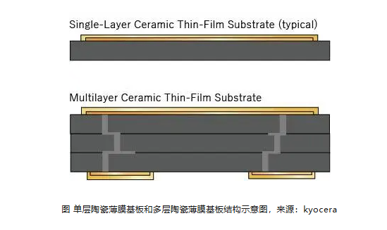
The HTCC stage primarily uses aluminum nitride green tape and tungsten metal paste as raw materials. Circuit patterns are formed by screen-printing metal paste onto the green tape, and electrical interconnection between layers is achieved through via filling. Subsequently, multilayer lamination is performed, followed by high-temperature co-firing (the AlN/W system typically requires around 1800°C or higher) and surface treatment to form a monolithic ceramic substrate with a 3D wiring structure. After grinding and polishing to obtain a flat, smooth ceramic surface meeting the roughness requirements for thin-film circuit fabrication, fine lines are created on the front and back surfaces of the HTCC substrate using thin-film processes.
The manufacturing process flow is as follows:
Paste Preparation
Mix raw materials such as ceramic powder, binder, plasticizer, and solvent according to the formula to prepare a stable and uniform casting slurry.
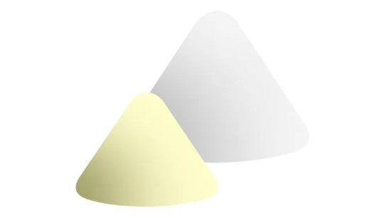
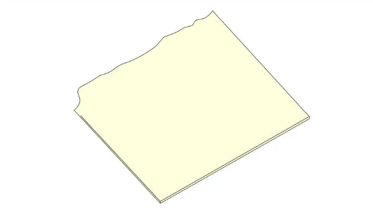
Tape Casting
Cast the slurry into a tape shape and dry it to produce green tapes with uniform thickness.
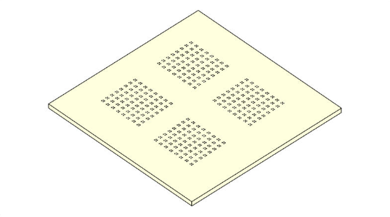
Via Punching/Filling
Process vias on the green tape and fill them with conductive paste to achieve interlayer electrical connections.
Screen Printing
Print circuit patterns on the surface of each green tape layer to form thick-film metallized routing.
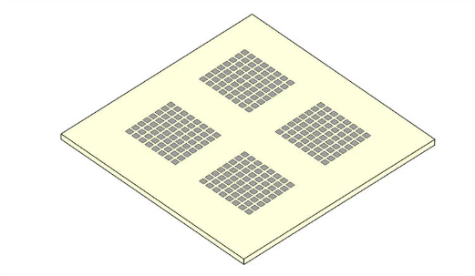
Lamination
Stack and press the printed green tapes according to design specifications to form a 3D circuit structure inside the ceramic substrate.
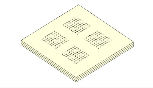
Cutting
Cut the laminated substrate into individual substrates for co-firing.
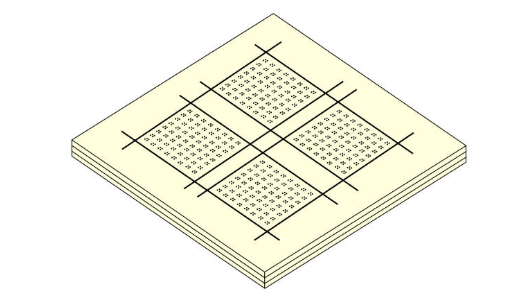
Co-firing
Fire individual substrates together in a high-temperature furnace to densify and integrate the ceramic and metallization layers.
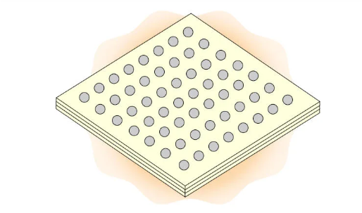
Grinding & Polishing
Grind and polish the surface of the co-fired ceramic substrate to ensure the flatness and surface finish required for subsequent thin-film deposition.
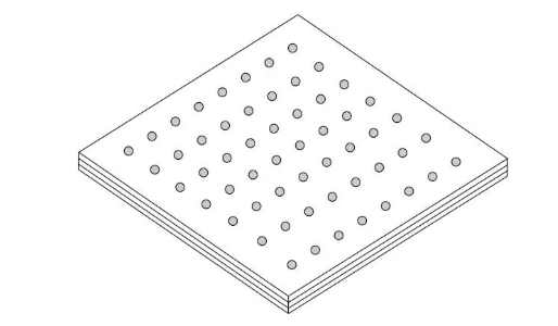
Thin-Film Deposition
Deposit thin-film metal layers on the substrate surface via evaporation or sputtering.
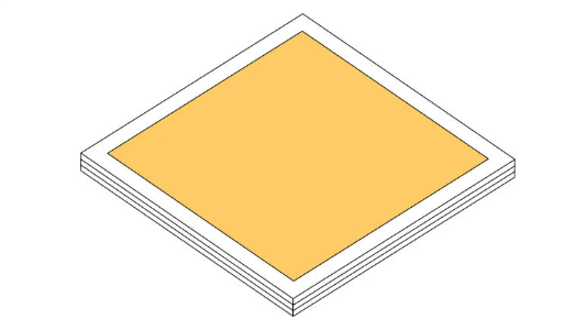
Photolithography
Apply photoresist to the substrate, then expose and develop it to form fine patterns.
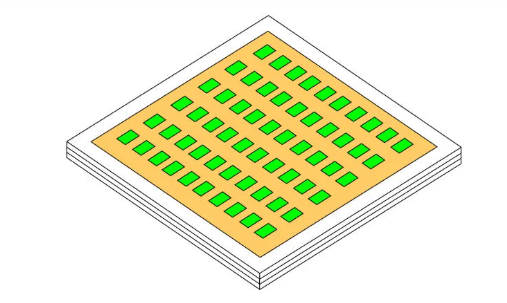
Etching
Remove unprotected metal areas via chemical etching, then strip the photoresist.
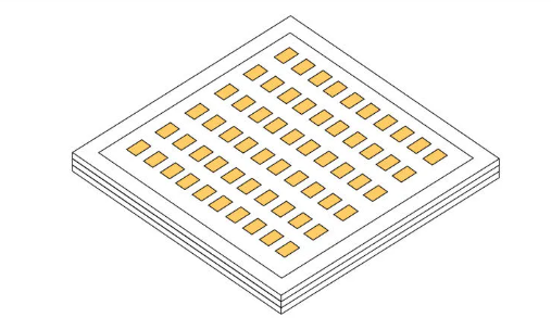
Electroplating
Thicken the metal layer using electroplating to reduce line resistance and improve solderability and reliability.
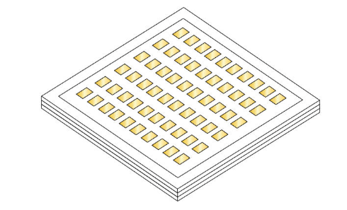
Cutting
Cut the substrate into individual units.
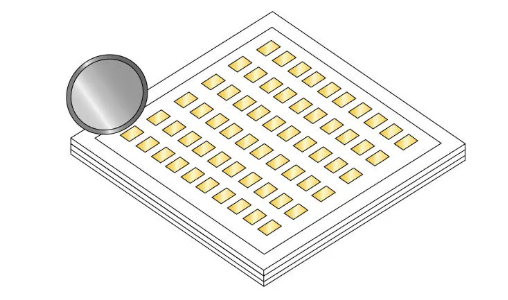
Inspection/Packaging/Shipment
After final inspection, package the finished substrates cleanly and ship them.
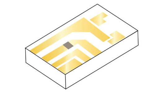
With the acceleration of AI computing power and data center construction, the optical communication market continues to grow. Ceramic thick/thin film substrates have been applied in 400G, 800G, and 1.6T high-frequency high-speed optical modules, playing important roles in scenarios such as microwave RF, power devices, and T/R assemblies, with market demand showing rapid growth.
trending news
Contact Us