



Sorry, no sales person is available right now to take your call. Pls leave a message and we will reply to you via email as soon as possible.
Home/ PCB News/ Embed First, Metallize Later: An Analysis of Low-Cost Embedded Ceramic PCB Technology
Embed First, Metallize Later: An Analysis of Low-Cost Embedded Ceramic PCB Technology
2026-10-08
To enhance the insulation and thermal dissipation performance of PCBs, ceramics can be embedded into the PCB substrate. Ceramics have a low coefficient of thermal expansion (CTE), which helps improve the dimensional stability of the PCB after embedding, meeting the requirements of high-precision surface mount components. Unlike the process of directly embedding metallized Active Metal Brazing (AMB) ceramic substrates, this article introduces a method for manufacturing ceramic-embedded PCBs: first embed the ceramic blocks, then perform one-time metallization on the entire board. Compared to using pre-metallized ceramic blocks, this approach reduces costs and facilitates better quality control of ceramic-embedded PCBs.
The specific process flow is as follows:
1. Inner Layer Substrate Pre-treatment and Lamination Windowing
Double-sided copper-clad laminates (CCL) are selected. Before lamination, complete the inner layer pattern fabrication: sequentially perform film application, exposure, development, and etching to obtain the inner layer circuits. Then stack them in the order of "substrate—prepreg—substrate," with the inner layer patterns facing the inside of the stack. After stacking, perform windowing at predetermined positions to form cavities for placing the ceramic blocks.
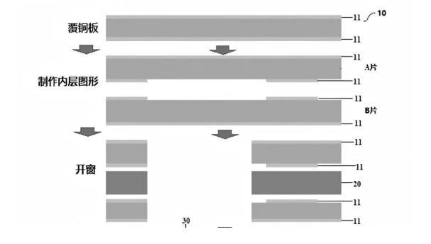
2. Embedding Non-Metallized Ceramic Blocks
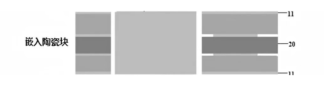
Place ceramic blocks without metal layers into the windowed openings. The ceramic blocks can be made of alumina, aluminum nitride, Low Temperature Co-fired Ceramic (LTCC), or a combination thereof. The dimensions of the ceramic blocks should be slightly smaller than the window size to allow for assembly clearance and facilitate subsequent prepreg flow filling.
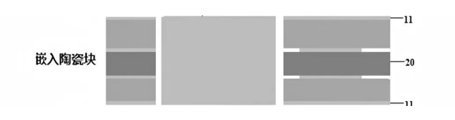
3. Lamination and Grinding/Planarization
Perform lamination on the stacked boards. During lamination, the prepreg melts and flows upon heating, bonding the upper and lower substrates and filling the gaps between the ceramic blocks and the windows. After lamination, grind/polish the board surface to planarize it, ensuring that the top surface of the ceramic blocks is flush with the outer surface of the substrate, guaranteeing flatness for subsequent metallization and pattern fabrication.
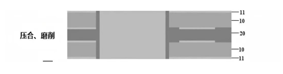
4. Full Board Surface Metallization
Perform metallization on the entire planarized board. First, prepare a conductive seed layer via vapor deposition (such as Physical Vapor Deposition, PVD), then electroplate copper to form an electroplated copper layer with a thickness of approximately 10–50 μm, creating a continuous metal layer on both the substrate surface and the ceramic block surface simultaneously. If necessary, clean, activate, or roughen the board surface before metallization to improve adhesion strength.
5. Fabricating Outer Circuit Patterns
Sequentially apply film, expose, develop, and etch the electroplated copper layer to fabricate the outer layer circuit patterns, ultimately obtaining the finished ceramic-embedded PCB.
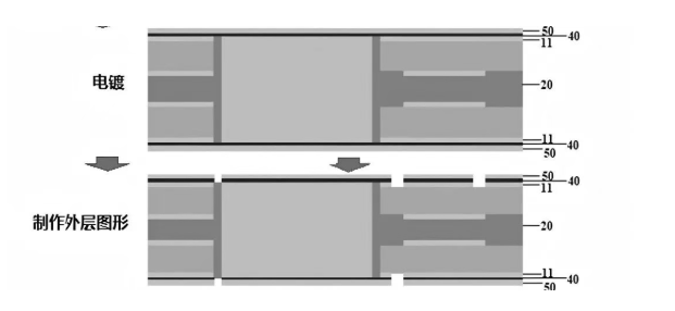
This method involves performing one-time metallization on the entire board after the ceramic blocks are embedded and planarized. Since the ceramic blocks do not require pre-metallization before embedding, material and processing costs are reduced, and potential damage to pre-metallized ceramic blocks during embedding and lamination is minimized, thereby improving process consistency and quality controllability of ceramic-embedded PCBs.
trending news
Contact Us