



Sorry, no sales person is available right now to take your call. Pls leave a message and we will reply to you via email as soon as possible.
Home/ PCB News/ High-Density Integrated Packaging Thermal Dissipation Breakthrough: Vertical Heat Dissipation Pathway of Chip-Copper Block-Copper Column-AMB Ceramic Substrate
High-Density Integrated Packaging Thermal Dissipation Breakthrough: Vertical Heat Dissipation Pathway of Chip-Copper Block-Copper Column-AMB Ceramic Substrate
2026-10-13
As the power density of high-performance CPUs, GPUs, FPGAs, and third-generation semiconductor power devices such as GaN continues to increase, the heat flux density per unit area rises significantly. Heat dissipation capability has become a critical factor limiting system performance, lifespan, and reliability. Traditional surface-mount technology directly solderes chips onto the PCB surface, requiring heat flow to pass through paths including solder, PCB dielectric, and vias, which results in long thermal paths and high thermal resistance. Although embedding copper blocks within the PCB can locally enhance thermal conductivity, it may still be constrained by high interface thermal resistance, CTE mismatch between copper and dielectric materials, and insufficient thermomechanical reliability.
This article proposes a vertical heat dissipation solution for high-density integrated packaging based on "Chip—Copper Block—Solid Copper-Plated Pillar—AMB Ceramic Substrate". This solution embeds pre-soldered copper blocks with chips inside multilayer boards and connects them to an AMB ceramic substrate at the bottom via solid copper-plated pillars, forming a low-thermal-resistance, primarily metal/ceramic vertical thermal conduction path. It provides a feasible engineering approach for improving heat dissipation and reliability in high-power-density devices.
1. Solution Overview
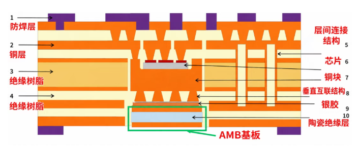
This solution integrates copper blocks with pre-soldered chips inside multilayer circuit boards and connects the bottom of the copper blocks to an AMB (Active Metal Brazing) ceramic copper-clad substrate via solid copper-plated pillars, constructing a vertical heat dissipation channel from the chip to the system-level heat sink. The core heat flow path can be summarized as:
Chip → Chip/Copper Block Solder Layer → Copper Block → Solid Copper-Plated Pillar → Silver Sintering Layer → AMB Top Copper Foil → Ceramic Substrate → AMB Bottom Copper Layer → System Heat Sink
This structure reduces the high thermal resistance caused by traditional PCB dielectrics and standard thermal vias. Meanwhile, it leverages the high thermal conductivity, high insulation, and relatively high mechanical strength of AMB ceramic substrates to improve heat spreading and thermomechanical reliability in high-power-density packaging.
2. Process Flow
2.1 Inner Core Board Milling and Pre-Embedding of Copper Blocks
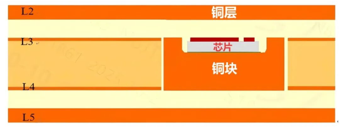
Milled slots are processed in corresponding areas of the PCB inner core layers, for example, forming Slot ① between L3—L4 layers. Pre-formed copper blocks are precisely embedded into the slots and secured, ensuring the top surface of the copper block is flush with the L3 layer surface. The top surface of the copper block must be firmly connected to the chip in advance via diffusion bonding or sintering processes to achieve efficient chip-level thermal coupling.
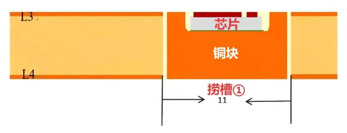
The key to this step lies in controlling the dimensional tolerance of the copper block, slot wall clearance, coplanarity, and chip soldering quality to ensure subsequent lamination filling and continuity of the thermal path.
2.2 First Multilayer Lamination
Prepreg sheets and copper foil are sequentially stacked on both sides of the core board with the embedded copper block. The first high-temperature, high-pressure lamination is performed to form the basic framework structure containing L2—L5 layers. During lamination, the resin in the prepreg must flow sufficiently to fill the gaps around the copper block, avoiding voids, delamination, and localized stress concentration.
2.3 Second Multilayer Lamination and Surface Treatment
The board after the first lamination undergoes a second stacking and lamination process, extending to L6 layers and above. Subsequently, laser opening and electroplating thickening are performed in the top area corresponding to the chip, followed by conventional PCB processes such as outer layer circuit pattern transfer, resulting in the formed multilayer board.
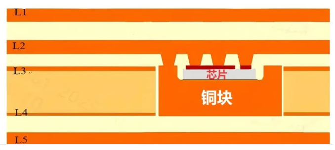
This stage requires balancing the thermal sensitivity of the already embedded chips and copper blocks. Lamination temperature, pressure, and heating/cooling rates must be controlled to avoid damaging the chips, interface solder layers, and copper block embedding structures.
2.4 Bottom Opening, Laser Drilling, and Preparation of Solid Copper-Plated Pillars
Opening milling is performed in the L5—L6 layer area directly below the copper block to form Slot ② for placing the AMB substrate. Subsequently, solid copper-plated pillars penetrating the dielectric layers are prepared at positions corresponding to the bottom of the copper block via laser drilling and electroplating hole-filling processes.
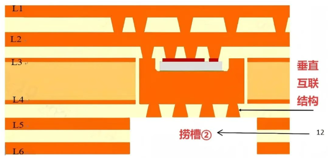
These solid copper-plated pillars serve as vertical interconnect structures, connecting to the bottom of the copper block at the upper end and exposed on the board surface at the lower end, providing a low-thermal-resistance metallic bridge for subsequent connection to the AMB substrate. Key process controls include the quality of laser-drilled hole walls, density of electroplated hole filling, void rate, and bonding strength between the copper pillars and the copper block.
2.5 AMB Substrate Assembly, Silver Sintering Bonding, and Insulation Filling
The AMB ceramic copper-clad substrate is precisely aligned and pre-positioned within the Slot ② window. A nano-silver film is placed between the bottom of the solid copper-plated pillar and the top copper foil of the AMB, ensuring tight contact among "Copper-Plated Pillar—Silver Film—AMB Copper Layer". Low-temperature silver sintering forms a dense metallurgical bond, integrating the AMB substrate into the multilayer board to achieve low thermal interface resistance.
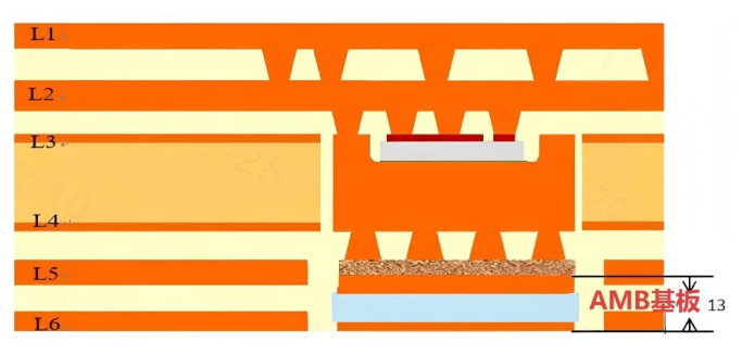
Subsequently, insulating resin is injected into the gap between the sidewalls of the AMB substrate and the inner walls of Slot ②. Once the resin fills the gap and fully cures, it achieves mechanical anchoring, electrical insulation of the sidewalls, and sealing protection for the AMB substrate. This step requires control over silver sintering temperature, pressure, time, and interface void rate, while ensuring compatibility between the insulating resin and the PCB dielectric, ceramic, and copper surfaces.
3. Advantages of the Solution
Low Thermal Resistance Vertical Heat Dissipation Path
By constructing a vertical thermal conduction path primarily consisting of metal and ceramics through "Chip—Copper Block—Solid Copper-Plated Pillar—AMB Ceramic Substrate", the thermal resistance introduced by traditional PCB dielectrics is reduced, facilitating rapid transmission of core heat to the system heat sink.
Improved Thermomechanical Reliability
AMB ceramic copper-clad substrates can utilize high-thermal-conductivity ceramic materials such as AlN and Si3N4, offering low CTE, high mechanical strength, and good insulation properties. Through reasonable stack-up and interface design, thermal expansion matching between high-power chips like Silicon and GaN and the package structure can be improved, reducing interface stress during thermal cycling.
Compatibility with High-Density Integrated Packaging
This solution embeds the heat dissipation structure within the multilayer board without significantly increasing the external volume of the system, making it suitable for the integrated packaging needs of high-density, high-power devices.
Reduced Junction-to-Ambient Thermal Resistance
With the assistance of a system-level heat sink, this vertical path effectively reduces the junction-to-ambient thermal resistance
Rth,j−a, enhancing the long-term reliability of high-power-density PCBs under harsh operating conditions.
4. Key Process Controls and Reliability Considerations
In engineering implementation, the following aspects require focused attention:
Dimensional matching, coplanarity, and embedding stability between the copper block and the core board slot;
Flow and filling capability of prepregs to avoid voids and delamination around the copper block;
Quality of laser drilling and electroplated hole filling, controlling hole wall defects and voids in copper pillars;
Density of silver sintering interfaces, void rate, and process compatibility with PCB materials;
Filling integrity, CTE matching, and heat resistance of insulating resin;
Verification of interface reliability under thermal cycling, high temperature/humidity, and power cycling.
5. Conclusion
The "Chip—Copper Block—Solid Copper-Plated Pillar—AMB Ceramic Substrate" vertical heat dissipation solution establishes a low-thermal-resistance metallic interconnection between embedded copper blocks and AMB ceramic copper-clad substrates, providing an engineering-feasible approach for heat dissipation in high-density packaging of high-performance CPUs, GPUs, FPGAs, and GaN power devices. While this solution shows potential in reducing thermal resistance and improving thermomechanical reliability, practical application still requires systematic optimization and verification considering specific material systems, stack-up structures, manufacturing capabilities, and reliability requirements.
trending news
Contact Us