



Sorry, no sales person is available right now to take your call. Pls leave a message and we will reply to you via email as soon as possible.
Home/ PCB News/ <div class="article-content"> <p>光模块PCB设计“分段金手指”主要基于以下几个关键原因:</p> <ul> <li><strong>信号完整性优化</strong>:高速差分信号(如10G/25G/40G/100G)对阻抗连续性要求极高。分段设计允许在不同区域独立控制阻抗匹配,减少反射和串扰。</li> <li><strong>电源与地隔离</strong>:将电源引脚、地引脚和信号引脚物理分离,可有效降低噪声耦合,提高信噪比(SNR),确保模拟前端(AFE)和数字逻辑的纯净供电。</li> <li><strong>机械可靠性与插拔寿命</strong>:分段结构可缓解整体应力集中,避免单一长条金手指在频繁插拔中因弯曲或磨损导致接触不良,提升连接器耐久性。</li> <li><strong>功能分区明确</strong>:便于按功能划分引脚组(如TX/RX数据对、I²C管理接口、电源VCC/GND、热插拔检测等),简化布线布局,降低交叉干扰风险。</li> <li><strong>兼容性与标准化</strong>:遵循MSA(多源协议)标准(如SFP+、QSFP28等),确保不同厂商模块间互操作性,同时支持未来速率升级时的引脚复用需求。</li> </ul> <p>简言之,“分段金手指”是高速光通信领域平衡电气性能、机械可靠性和标准化要求的工程最优解。</p> </div>
<div class="article-content"> <p>光模块PCB设计“分段金手指”主要基于以下几个关键原因:</p> <ul> <li><strong>信号完整性优化</strong>:高速差分信号(如10G/25G/40G/100G)对阻抗连续性要求极高。分段设计允许在不同区域独立控制阻抗匹配,减少反射和串扰。</li> <li><strong>电源与地隔离</strong>:将电源引脚、地引脚和信号引脚物理分离,可有效降低噪声耦合,提高信噪比(SNR),确保模拟前端(AFE)和数字逻辑的纯净供电。</li> <li><strong>机械可靠性与插拔寿命</strong>:分段结构可缓解整体应力集中,避免单一长条金手指在频繁插拔中因弯曲或磨损导致接触不良,提升连接器耐久性。</li> <li><strong>功能分区明确</strong>:便于按功能划分引脚组(如TX/RX数据对、I²C管理接口、电源VCC/GND、热插拔检测等),简化布线布局,降低交叉干扰风险。</li> <li><strong>兼容性与标准化</strong>:遵循MSA(多源协议)标准(如SFP+、QSFP28等),确保不同厂商模块间互操作性,同时支持未来速率升级时的引脚复用需求。</li> </ul> <p>简言之,“分段金手指”是高速光通信领域平衡电气性能、机械可靠性和标准化要求的工程最优解。</p> </div>
2026-10-15
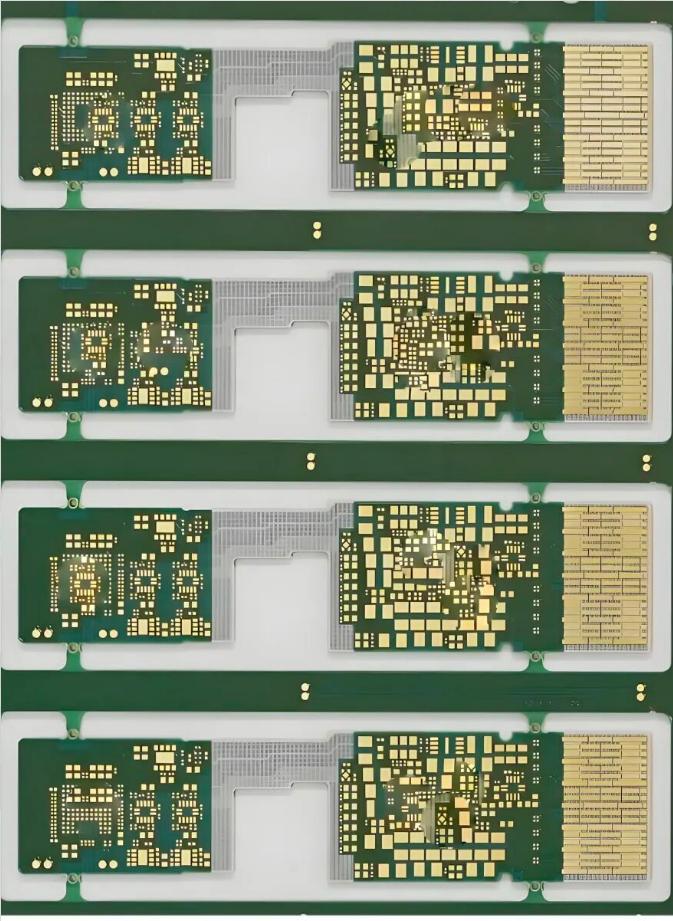
Optical modules are high-speed communication devices that perform optical-to-electrical and electrical-to-optical conversion. Typical products consist of optical components, electrical chips, PCBs, structural parts, and heat dissipation elements. The PCB edge is inserted into one end of devices such as switches and servers, typically featuring gold-plated contact areas, commonly known as "gold fingers." The so-called "segmented gold fingers" are not merely an aesthetic design choice; rather, they involve layout and isolation of contact areas based on different electrical functions, potentially achieving timing control through contacts of varying lengths. This involves signal integrity, power integrity, hot-swap timing, mechanical fit, and manufacturability for mass production.
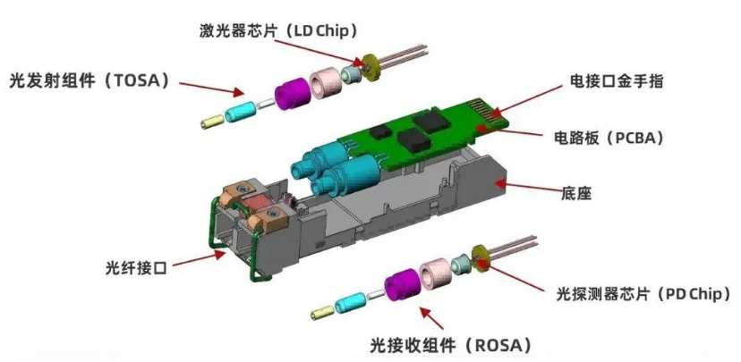
(Figure: Illustration of edge gold fingers/segmented gold fingers on an optical module PCB)
I. Typical Characteristics of Optical Modules
High Speed and High Frequency
Data rates have evolved from 1G/10G and 25G/100G to 200G/400G/800G or even higher, imposing stringent requirements on signal integrity, power integrity, and high-speed interconnects.
Opto-Electronic Hybrid
It incorporates both optical and electronic functions, involving devices such as lasers/modulators, photodetectors, DSPs, CDRs, drivers, and TIAs. Its manufacturing processes and testing possess cross-disciplinary characteristics.
High Density and Miniaturization
Common packages include SFP, SFP28, QSFP, QSFP-DD, and OSFP. Products must integrate high-speed circuits, optical components, and heat dissipation structures within limited volume.
Sensitivity to Thermal Management
Increased power consumption of high-speed chips and optoelectronic devices makes heat dissipation paths, thermal resistance, temperature rise, and device operating temperatures critical design factors.
High Reliability Requirements
Products generally need to meet the long-term operation requirements of communication equipment, thus focusing on temperature cycling, humidity, mechanical stress, insertion/extraction lifespan, and high-speed electrical performance.
High Degree of Standardization
Mechanical dimensions, electrical interfaces, management interfaces, and optical interfaces are usually constrained by standards or industry specifications such as MSA, IEEE, and OIF. Product design has strong standard compatibility requirements.
It should be noted that optical modules with different speeds, package forms, and application scenarios vary significantly in chip composition, optical architecture, power consumption, and manufacturing difficulties. The above characteristics should not be viewed as fixed configurations for all optical modules.
II. Why Are Gold Fingers "Segmented"?
The core purpose of segmented gold fingers is to layout and isolate contact areas according to different electrical functions, while balancing high-speed performance, power return paths, and insertion/extraction timing. Key considerations include:
Differentiation of Electrical Functions
High-speed differential signals, power, ground, and low-speed control/management signals need to be arranged according to interface definitions, resulting in distinct contact zones on the gold fingers.
Reducing Coupling Between High-Speed Signals
Proper arrangement of signal, ground, and power pins helps control crosstalk and return paths for high-speed interfaces, reducing electromagnetic coupling between adjacent signals.
Improving Signal Integrity
High-speed differential pairs require maintained impedance continuity and reasonable return paths. The arrangement, dimensions, spacing, and reference ground design of contact areas all affect the SI performance of the interface.
Insertion/Extraction Timing Control
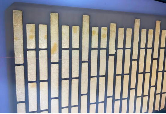
Some interfaces utilize contacts of different lengths to create timing, ensuring that ground, power, and signals establish or disconnect connections in a prescribed order. A typical principle is to establish ground reference first, then connect power, and finally establish signals; the reverse order applies during extraction. Specific sequences should follow the corresponding interface standard to avoid undesired electrical states during insertion/extraction.
Enhancing Contact Reliability
Different pins have varying requirements for contact resistance, wear resistance, plating quality, and insertion/extraction lifespan. Therefore, the structure and surface treatment of gold fingers must match the connector.
Therefore, a more accurate engineering understanding of segmented gold fingers is: satisfying high-speed electrical performance, power/ground return paths, and insertion/extraction timing requirements simultaneously through functional zoning of contacts, geometric dimensions, and necessary length differences.
III. Main Manufacturing Challenges
The true difficulty lies not in producing gold fingers, but in stably translating design requirements into mass production capability under conditions of high density, high speed, and high reliability.
Dimensional and Positional Accuracy of Gold Fingers
Gold fingers involve multiple dimensional requirements including trace width, spacing, length, chamfering, edge position, and board thickness. Tolerances in PCB manufacturing processes such as etching, plating, forming, and outline processing can cause cumulative deviations. For high-speed optical modules, positional deviation of contacts may further affect connector mating and high-speed channel performance.
Gold Plating Quality and Insertion/Extraction Durability
Gold fingers typically require good wear resistance and contact reliability, necessitating control over plating thickness, uniformity, surface cleanliness, adhesion quality between the gold layer and underlying metal, and surface defects such as scratches, pits, and exposed copper. During mass production, factors like board edge position, current distribution, and fixture contact may cause plating uniformity issues, ultimately manifesting as changes in contact resistance after insertion/extraction cycles.
Process Window for Segmented Areas
Segmented gold fingers often accompany different lengths, functional zones, and smaller spacings. Manufacturing requires simultaneous control of pattern accuracy, plating uniformity, and forming precision. The process window is typically more sensitive than that for simple, regular contacts.
Manufacturing Consistency for High-Speed Signals
As optical modules enter high-speed iterations like 100G/400G/800G, PCB manufacturing cannot just focus on "continuity." Process variations in dielectric thickness, dielectric constant, copper thickness, trace width/spacing, and etch undercutting can affect metrics such as impedance, insertion loss, and return loss. Therefore, manufacturing must link PCB process capability with SI requirements.
Coordination of Multiple Materials and Processes
Optical modules are rarely just a single PCB manufacturing issue; they also involve mounting optical components, chip placement/soldering, connectors, structural parts, and heat dissipation materials. Different materials have varying CTEs, thermal conductivity, and mechanical properties, which can lead to warpage, stress, or thermal reliability issues after assembly.
High-Density Assembly and Yield
Small product dimensions and high device density result in tight coupling between SMT, precise placement, soldering, optical coupling, and testing processes. Minor deviations in one process may only be revealed in subsequent optical or high-speed electrical performance tests. Thus, process yield, failure localization, and test coverage are significant challenges for mass production.
IV. Summary
The core manufacturing challenge for optical modules is to ensure high-speed electrical performance, optical performance, heat dissipation, mechanical fit, and long-term reliability within limited dimensions, while converting various design tolerances into stable mass production capabilities.
Segmented gold fingers primarily serve interface function zoning, high-speed signal integrity, power/ground return paths, and insertion/extraction timing. Manufacturing focuses on dimensional accuracy, plating quality, insertion/extraction durability, high-speed impedance/loss control, and overall assembly yield. The specific segmentation method, contact lengths, and plating requirements are typically determined comprehensively based on package form, connector definition, and standards such as MSA/IEEE/OIF.
trending news
Contact Us