



Sorry, no sales person is available right now to take your call. Pls leave a message and we will reply to you via email as soon as possible.
Home/ PCB News/ In-depth Reliability Control Standards for High-Order HDI (High Density Interconnect) Printed Circuit Boards
In-depth Reliability Control Standards for High-Order HDI (High Density Interconnect) Printed Circuit Boards
2026-10-08
Current market-standard HDI inspection criteria are largely limited to superficial dimensions such as visual appearance, basic continuity, and routine cross-section analysis. They fail to effectively identify inherent latent failure risks in high-end products, including but not limited to: intermittent opens induced by thermal cycling, hidden micro-cracks in vias, filled-via delamination, interface voids, impedance drift, Conductive Anodic Filament (CAF) migration, and board blistering during secondary SMT reflow—key failure modes affecting mass production and end-use reliability.
This specification is built upon IPC-2226, IPC-6012, and IPC-6018 as its technical framework. It systematically deepens and upgrades requirements for critical root causes that are insufficiently constrained in current IPC standards, often compromised during manufacturing cost reduction, and exhibit an end-use failure reproduction rate exceeding 90%. This standard applies to supplier qualification, incoming material full-inspection decisions, process audits, and mass-production failure traceability, possessing the highest level of technical judgment authority.All clauses represent zero-tolerance red lines; any single non-conformance results in rejection of the entire batch (Reject), immediate batch quarantine, and mandatory initiation of 8D closed-loop corrective action.
I. Red Lines for Micro-Via Laser Drilling Control
——The Source of 80% Reliability Failures in High-End HDI
1.1 Residue Glue and Burn Marks at Via Bottoms (Invisible Fatal Defects)
IPC Traceability: IPC-6018 §4.4.3, IPC-A-600 §8.3 (Mandatory cleanliness requirements for via bottoms; typically exempted in conventional standards but strictly enforced for high-reliability high-end products)
Routine inspections do not cover this item, yet it is the primary cause of intermittent opens in micro-vias. Under thermal cycling stress, defect layers at the via bottom tend to crack, leading to resistance drift and intermittent circuit connectivity, ultimately causing functional anomalies in end products.
Red Line Requirements:
Via bottoms mustabsolutely prohibitthe presence of carbonized thin layers, micro-crystalline residue glue, or laser-burnt blackened layers. Zero residue tolerance.
The copper surface at the via bottom must exhibit a uniform metallic original color, free from mottling, localized over-burning whitening, or fog-like contamination. Copper surface consistency must reach 100%.
Laser drilling energy must precisely match process parameters: excessive energy embrittles the substrate, inducing micro-cracks; insufficient energy fails to remove residue glue completely, embedding latent defects. Parameter deviation out of control is prohibited throughout the process.
Red Line Judgment: If cross-section inspection reveals any blackening, fog-like coating, or carbonized residue at the via bottom, it is judged as a fatal defect, resulting in rejection of the entire batch.
1.2 Micro-Cracks on Via Walls (Highly Concealed, Difficult to Detect)
IPC Traceability: IPC-6012 Class3 §5.2.1, IPC-2226 §7.3 (Mandatory zero-crack specification for high-reliability micro-via walls)
Micro-via walls enforce zero-crack tolerance, comprehensively prohibiting all forms of cracks including hairline micro-cracks, corner micro-cracks, and entry-edge chipping. The corner areas of via openings in second-order and third-order stacked vias are high-risk zones for crack occurrence and require focused inspection.
Such micro-cracks are invisible to the naked eye but continue to propagate after ≥500 thermal cycles, eventually causing micro-via opens and circuit failures.
Mandatory Rule for High-End Products: The crack tolerance for via walls in all stacked layer levels is 0, with no process exemptions. Uniform execution is required for both Class2 and Class3 products.
1.3 Hard Red Line for Micro-Via Aspect Ratio
IPC Traceability: IPC-2226 §6.2, IPC-6018 §4.4.1 (Mandatory maximum aspect ratio standard for HDI laser micro-vias)
For all laser micro-vias in first, second, and third orders, the aspect ratio is strictly controlled at ≤1.0:1.0 (precision retained to 1 decimal place). Any excess beyond this limit for any batch or structure is strictly prohibited. For automotive/server high-reliability products, ≤0.75:1.0 is preferred.
If the manufacturing process arbitrarily exceeds the aspect ratio to improve routing density, it results in thick copper plating at the top and thin at the bottom, uneven bottom plating, and hidden broken copper at the via bottom. This inevitably leads to failure under thermal conditions, completely violating IPC process reliability requirements.
II. Depth Control Red Lines for Stacked Vias
——Core Proprietary Control Domain for High-End HDI
2.1 Stacking Alignment Accuracy and Overlap Reliability (Common Industry Cost-Cutting Point)
IPC Traceability: IPC-6012 Class2/Class3 §5.3.2, IPC-2226 §7.4.2 (Grading standard for stacked micro-via alignment deviation)
Class 2 (General Grade): Stacked via alignment offset ≤25.0μm;
Class 3 (Automotive/Server High-Reliability Grade): Alignment offset ≤15.0μm (precision retained to 1 decimal place).
Absolutely ProhibitedSingle-side suspension, single-side partial overlap, or half-contact stacked structures. These structures appear conductive externally but actually have only partial contact. They are prone to delamination and open circuits under thermal expansion/contraction, constituting defective non-full-overlap structures explicitly prohibited by IPC.
2.2 Restrictions on Multi-Layer Stacked Structures (Major Manufacturer High-End Process Ban)
IPC Traceability: IPC-2226 High-Reliability Stacked Structure Appendix, IPC-9701 Thermal Cycling Reliability Specification
Three-layer vertical direct-through stacking without buffer is prohibited. This structure concentrates stress to extreme levels, inevitably causing cracking under temperature cycling, exceeding the scope of IPC reliable structural design.
Third-order HDI productsmust adopt an "interleaved stacking + local buffer layer" optimized structure to disperse stress and meet IPC long-term reliability requirements.
Automotive-grade high-reliability productscompletely prohibit two-layer or higher direct-through stacking. Interleaved transition stacking processes must be used to avoid stress concentration and comply with AEC-Q200 automotive reliability baselines.
2.3 Copper Thickness Gradient Uniformity Standard for Stacked Vias (Deep Core Control Item)
IPC Traceability: IPC-6012 Class3 §5.4.3, IPC-A-600 §8.4 (Requirements for micro-via copper plating thickness and uniformity)
Typical process defects manifest as thick copper at the via mouth and thin at the bottom, representing typical latent defects. Qualified high-end plating must ensure uniform copper thickness throughout the via, with no gradient deviation.
Excellent Process Standard: Uniform copper plating thickness throughout the micro-via is controlled within 18.0–25.0μm(precision retained to 1 decimal place).
Fatal Defect Judgment: Via bottom copper thickness <12.0μmindicates extremely high risk of hidden broken copper and resistance drift, failing to meet the IPC minimum copper plating thickness baseline.
III. Red Lines for Resin-Filled Via Depth Control
——Items Prone to Fraud and High Customer Complaints
3.1 Zero-Tolerance Specification for Internal Voids in Filled Vias
IPC Traceability: IPC-6018 §5.5.2, IPC-2226 §8.3 (Resin-filled via void control; upgraded to zero tolerance for high-end products)
Routine inspection only checks the surface of filled vias. This specification deepens to the cross-sectional core, enforcing zero internal void tolerance. All internal defects, including central micro-voids, interlayer gap voids, edge linear voids, and delamination-type pores, are comprehensively prohibited. This breaks through conventional IPC sampling tolerance standards to achieve zero-defect full inspection.
Defect Hazard: During high-temperature secondary SMT reflow, gases in internal voids expand, causing board bulging, substrate blistering, BGA soldering voids, and other batch defects and end-product failures.
3.2 True Flatness Control of Filled Vias (Preventing Artificial Grinding Fraud)
IPC Traceability: IPC-6012 §5.5.1 (Baseline for filled via surface flatness; this standard tightens high-end control thresholds)
True depression depth of micro-via filling≤10.0μm(measured true value from cross-section, precision retained to 1 decimal place, excluding illusions caused by grinding/polishing).
It is strictly prohibited to mask depression defects through grinding and polishing. Indicators of grinding fraud include locally thin copper layers, disordered board texture, and uneven copper thickness distribution. Detection of these signs results in immediate rejection.
3.3 Bonding Reliability Between Resin and Via Wall Interface
IPC Traceability: IPC-2226 §8.4, IPC-9703 Moisture Insulation Reliability Specification
The bonding interface between resin and copper via wall must be tightly adhered, free of gaps, peeling seams, or black-edge defects. Black edges at the interface indicate early-stage micro-peeling, which forms channels for moisture penetration. Long-term exposure to humid heat conditions can lead to insulation degradation, micro-leakage, and circuit failure, violating IPC interface bonding integrity requirements.
IV. Red Lines for Latent Defects in Buildup Layer Lamination
——Primary Cause of Board Blistering in High-End Products
4.1 Control of PP Resin Content Distribution Around Micro-Vias
IPC Traceability: IPC-2226 §9.2 (Baseline for buildup layer resin filling integrity control)
All areas around micro-vias must be fully filled with resin, with no lack of resin, lean resin, or uneven resin content. Lack of resin in dense BGA routing areas is the starting point for interlayer micro-delamination, directly inducing later-stage blistering and delamination failures, constituting a clear lamination structural hazard defined by IPC.
4.2 Alignment Deviation and Resin Shrinkage Control for Multi-Layer Buildups
IPC Traceability: IPC-6012 Class3 §6.2.1 (Cumulative alignment deviation control requirements for multi-layer buildups)
Alignment deviation for a single buildup layer ≤15.0μm; cumulative deviation for multiple layers is strictly prohibited from exceeding limits (precision retained to 1 decimal place).
Layer compression/shrinkage causes uneven dielectric layer thickness, directly leading to impedance drift, signal integrity anomalies, and high-speed signal distortion, failing to meet IPC high-speed board material dielectric consistency requirements.
4.3 Zero Tolerance for Interlayer Interface Micro-Delamination
IPC Traceability: IPC-A-600 §9.3, IPC-9701 Thermal Cycling Delamination Judgment Standard
Under grayscale cross-section inspection, interlayer interfaces must be uniform and continuous, free from fine lines, black lines, gaps, or other anomalies. Black lines at the interface indicate early-stage micro-delamination defects, which can cause interlayer separation and board blistering after just ≥3 reflow cycles, constituting a fatal IPC lamination defect.
V. Excessive Etching Depth Control for Traces
——Specialized Specification for High-Frequency High-Speed HDI
5.1 Verticality of Trace Sidewalls (Core Guarantee for SI Signal Integrity)
IPC Traceability: IPC-2226 §10.3, IPC-6012 §7.2 (Control of etching profile for high-speed traces)
Severe trapezoidal etching, undercutting, and excessive lateral etching are strictly prohibited. Excessive lateral etching causes impedance fluctuations, excessive differential pair impedance mismatch, and EMI anomalies, directly impacting transmission stability in high-frequency high-speed circuits and failing to meet high-speed SI signal integrity IPC baselines.
5.2 Critical Width Control Red Line for Fine Traces
IPC Traceability: IPC-6012 Class3 §7.1.2 (Tolerance deviation for fine trace width)
For 0.075mm ultra-fine traces, residual trace width must not fall below 85.0%of the design value (percentage precision retained to 1 decimal place). Local widths falling below this limit are prone to fatigue fracture under long-term power application, leading to open circuit failures.
5.3 Control of Trace Copper Plating Crystallization and Surface Defects
IPC Traceability: IPC-A-600 §7.3, IPC-6012 §5.4 (Conductor surface integrity requirements)
Trace copper surfaces must be smooth and dense, free from pinholes, crystallization voids, or protruding plating particles. Pinholes, when exposed to moisture, induce CAF (Conductive Anodic Filament) growth, ultimately leading to interlayer leakage and short-circuit failures.
VI. Deep Control of CAF (Conductive Anodic Filaments)
——Killer Factor for Long-Term Reliability
IPC Traceability: IPC-9703 §5.2, IPC-6012 Long-Term Insulation Reliability Appendix (Not mandatorily enforced in conventional standards; zero tolerance for high-end)
Conventional industry standards lack specific clauses, but CAF migration is among the TOP3 core causes of long-term end-product failures.
Interlayer dielectric substrates must befree of cracks and resin fiber damage, eliminating CAF growth channels and meeting IPC dielectric integrity requirements.
Between through-holes and among dense micro-vias,filamentous copper migration and ion precipitation are strictly prohibited.
Under humid heat environments plus long-term voltage bias, continuous CAF growth leads to intermittent conduction anomalies and hidden faults such as nighttime device crashes.
Mandatory high-end requirement: All micro-via dense areas and BGA core regions must satisfy negative CAF requirements, with no migration channels allowed. Control levels significantly exceed conventional IPC standards.
VII. Red Lines for Electrical Performance Deep Control
——Covering Continuity and Latent Resistance Drift
7.1 Consistency Control of Micro-Via Conduction Resistance
IPC Traceability: IPC-6012 Class3 §8.2.1 (Consistency deviation requirements for micro-via conduction resistance)
For micro-vias of the same batch, structure, and layer level, therange of conduction resistance must be ≤3.0mΩ(precision retained to 1 decimal place). Excessive resistance dispersion indicates batch-level hazards such as thin via copper, hidden micro-cracks, or poor interface contact.
7.2 Control of Latent Leakage Current Under High Temperature and Humidity
IPC Traceability: IPC-9703 Damp Heat Insulation Test Standard, IPC-6012 High-Reliability Electrical Aging Requirements
Based on passing room-temperature electrical tests, products must complete an 85°C / 85%RH high-temperature high-humidity 48h aging test. Post-aging withstand voltage tests must show no leakage, and insulation resistance must meet standards. This thoroughly eliminates issues like low-temperature freezing or functional anomalies caused by micro-leakage under high-temp/humid conditions despite normal room-temp performance, covering blind spots in conventional IPC room-temperature testing.
VIII. Deep Control Standards for SMT Process Compatibility
——Rare Control Items on the Manufacturing Side
8.1 Specialized Control of Local Warpage in BGA Areas
IPC Traceability: IPC-6012 §10.2, IPC/JEDEC J-STD-005 Board Warpage Control (High-end tightening of local area thresholds)
Conventional standards only control overall board warpage. High-end products focus on controlling local warpage in core functional areas. Board surface warpage within a 5mm range of a single BGA area must be ≤0.30% (percentage precision retained to 2 decimal places). Exceeding this tolerance directly leads to batch defects such as SMT solder voids, cold joints, and false contacts.
8.2 Control of Filled Via Concavity/Convexity for SMT Printing Compatibility
IPC Traceability: IPC-2226 §8.5 (Baseline for adapting filled via morphology to assembly processes)
Excessive concavity → Insufficient solder paste deposition, leading to false contacts and inadequate reliability.
Excessive convexity → Lifts the stencil, causing uneven solder paste printing and misalignment, resulting in batch SMT welding defects.
Both items must be strictly controlled within the process window to meet IPC structural baseline requirements for SMT process compatibility.
IX. Exclusive Control Bans for Automotive & Server High-End Applications
——Compliant with AEC-Q200 / IATF16949
Traceability Note: Based on dual upgrades from IPC-6012 Class3 high-end baseline + AEC-Q200 automotive grade + IATF16949 process quality system.
For high-reliability scenarios such as automotive and servers, new exclusive zero-tolerance bans are added to fully align with automotive and industrial high-reliability certification systems:
Prohibitcontinuous stacked arrays of dense micro-vias to avoid cracking due to local stress concentration, complying with IPC stress optimization design specifications.
All buildup layer dielectric substrates must have a TG Value ≥180°C. Mixing with low-TG substrates is strictly prohibited to eliminate risks of high-temperature delamination and blistering, exceeding conventional IPC general baselines.
Strictly Prohibitthe use of recycled PP sheets, recycled resins, recycled fillers, or other regenerated raw materials to prevent substandard performance, satisfying IATF16949 raw material traceability controls.
Products must pass ≥1500 thermal cycle testswith no resistance drift, no cracks, and no delamination throughout, far exceeding the conventional IPC-9701 baseline of 500 cycles.
All products must implement 100% cross-section inspectionfor BGA core areas. Sampling is prohibited; full coverage screening for latent defects is required, exceeding conventional IPC sampling levels.
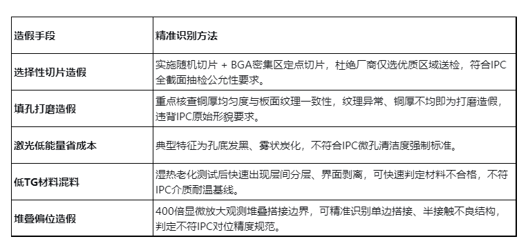
X. Guide to Identifying Supplier Process Fraud and Cost-Cutting
——Audit Tool Dedicated for SQE
Traceability Basis: Formulated by combining IPC compliance baselines with high-frequency risks of mass-production process fraud, providing specialized judgment criteria for incoming material audits and process reviews.
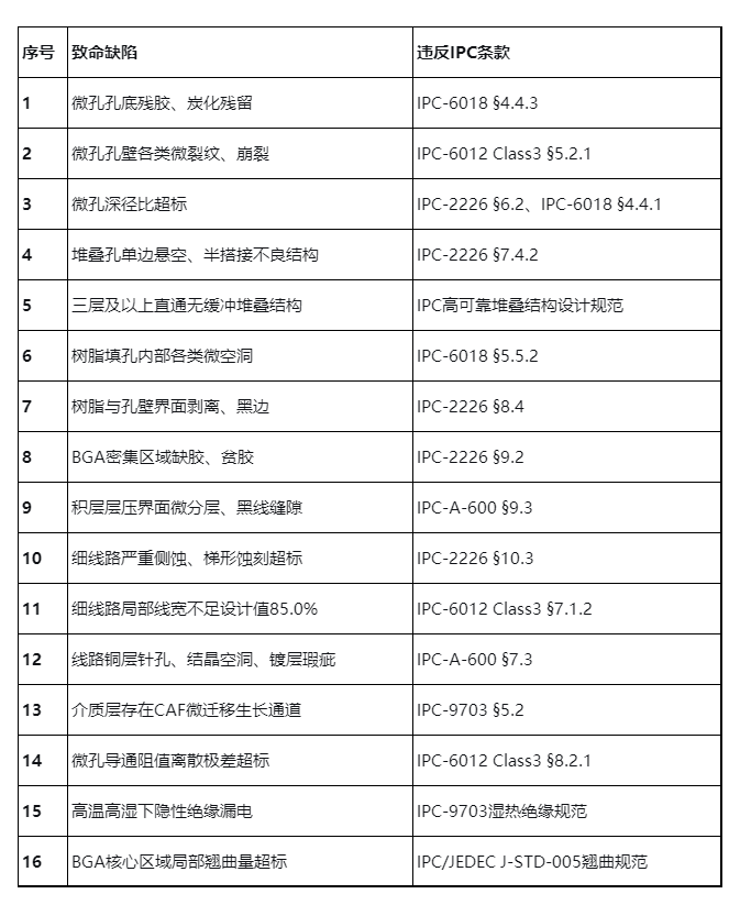
XI. Ultimate Zero-Tolerance List of 16 Fatal Defects for High-End HDI
Overall Traceability: Each item represents a violation of IPC standard baselines combined with root causes of latent mass-production failures. Detection results in whole-batch rejection, batch quarantine, and initiation of 8D traceability.
trending news
Contact Us