



Sorry, no sales person is available right now to take your call. Pls leave a message and we will reply to you via email as soon as possible.
Home/ PCB News/ <p>What is UHDI or Ultra HDI PCB? How does ultra-high density interconnect technology work?</p>
<p>What is UHDI or Ultra HDI PCB? How does ultra-high density interconnect technology work?</p>
2026-09-24
Ultra High Density Interconnect (UHDI) PCBs are printed circuit boards that have evolved from High Density Interconnect (HDI) technology. They further increase PCB density, allowing components to be placed more closely together, thereby reducing the overall board size. UHDI pushes the boundaries of PCB and semiconductor device manufacturing capabilities, representing a significant advancement in miniaturization and integration, enabling electronic components and systems to achieve extremely high functional integration within smaller footprints.
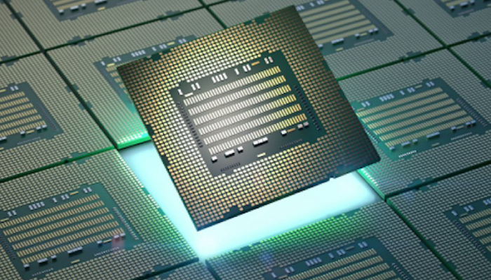
UHDI technology enables finer traces and smaller vias/microvias while significantly increasing interconnect density, resulting in higher signal integrity and lower PCB power consumption. UHDI trace widths and spacing are typically less than 1 mil (0.001 inch), which necessitates shifting measurement units from mils to micrometers. Since 1 mil equals 25 micrometers, UHDI refers to traces and spacing on printed circuit boards below 25 micrometers.
According to the definition established by the IPC working group, UHDI PCBs typically possess the following characteristics:
Conductor/trace width and isolation distance less than 50 µm;
Dielectric thickness less than 50 µm;
Microvia diameter less than 75 µm;
Product features exceeding current IPC 2226 Class C standards.
UHDI PCB Design
UHDI PCBs can be rigid or flexible and typically employ multi-layer structures to meet high-density interconnect requirements. As electronics continue to miniaturize, printed circuit boards shrink not only in the X-axis but also in the Y-axis. Although multilayering is crucial for maintaining signal integrity and reducing electromagnetic interference in UHDI PCBs, designers can integrate traces into fewer layers through fine-line routing, thereby reducing the number of HDI build-up layers. Reducing HDI build-up layers significantly lowers PCB manufacturing costs and helps offset some of the additional expenses associated with acquiring ultra-high-density interconnect manufacturing capabilities.
High-performance substrate materials, such as Ajinomoto Build-up Film (ABF), BT epoxy resin-based materials, thin liquid crystal polymers (e.g., UltraLam), and resin-coated copper films (such as metallized polyimide, pure polyimide, and cast polyimide), serve as alternatives to laser-drillable materials and thin reinforced FR4. These materials can be combined to construct ultra-high-density interconnect structures. A typical combination involves using BT epoxy resin-based copper-clad laminates as core substrates with traditional buried vias, and employing ABF as outer build-up layers to support fine-line routing. This build-up method has been used for organic substrates in BGA packages, and the same approach can be applied to ultra-high-density interconnect PCBs.
Challenges in UHDI PCB Manufacturing
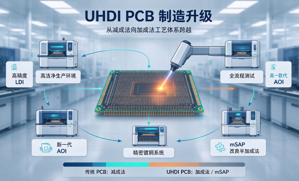
Every major technological advancement brings manufacturing challenges. UHDI represents not just a significant change, but a quantum leap in technology. It signifies a fundamental shift in PCB manufacturing methods, moving from traditional subtractive processes to additive processes. Simultaneously, it requires not only new manufacturing methods but also new equipment, chemicals, materials, and inspection capabilities.
In the past, UHDI PCB manufacturing capabilities were generally cost-effective only at very high volumes, thus primarily applied to certain high-computing consumer products and IC production with higher I/O counts. Today, as global access to these advanced capabilities expands, more designers can utilize them even at lower volumes or during prototyping stages. This also means that many advanced components previously reserved for high-volume consumer devices can now be used at lower volumes. Consequently, UHDI capabilities are becoming increasingly accessible to low-volume manufacturers.
PCB manufacturers producing ultra-high-density interconnect boards must meet stricter requirements regarding equipment and manufacturing environments. To enable factories to manufacture ultra-high-density interconnect boards, substantial upgrades are necessary, involving investments in equipment and processes during the manufacturing stage. Upgrades required for manufacturing ultra-high-density interconnect circuit boards include:
State-of-the-art Laser Direct Imaging (LDI) equipment;
Extremely clean production environments;
More comprehensive and rigorous testing;
Latest Automated Optical Inspection (AOI) equipment;
Newest copper plating equipment and chemicals;
New processes, such as mSAP (modified Semi-Additive Process);
Newer, cleaner, and more uniform materials.
Advantages of UHDI PCBs
UHDI PCBs offer significant advantages, particularly in reducing the weight and size of electronic devices while maintaining high performance. Their ability to accommodate more components in compact spaces increases component density, making them ideal for advanced electronic applications. Furthermore, UHDI PCBs improve electrical performance by shortening distances and electrical paths between components, thereby reducing signal loss, parasitic capacitance, and inductance. This facilitates better signal integrity and faster signal transmission. Additionally, their multi-layer structure and complex routing capabilities provide greater design flexibility, enabling the development of more innovative and sophisticated electronic products.
Applications of UHDI PCBs
UHDI is transforming numerous industries through "miniaturization without compromising performance." Key application areas include:
Consumer Electronics: Smartphones, tablets, and wearable devices achieve high performance in compact designs through UHDI.
Automotive Electronics: Advanced Driver Assistance Systems (ADAS), Electric Vehicle (EV) power electronics, and infotainment systems leverage UHDI to enhance reliability and efficiency.
Medical Devices: UHDI enables highly compact and precise medical electronics, such as imaging systems and implantable devices.
Aerospace and Defense: UHDI technology enhances performance and reliability in mission-critical applications like radar systems, avionics, and satellite communications.
trending news
Contact Us