



Sorry, no sales person is available right now to take your call. Pls leave a message and we will reply to you via email as soon as possible.
Home/ PCB News/ Blind Vias, Buried Vias, Through-Holes: Differences and HDI 1st-3rd Order/Any-Layer Determination
Blind Vias, Buried Vias, Through-Holes: Differences and HDI 1st-3rd Order/Any-Layer Determination
2026-09-22
In PCB design and manufacturing, many hardware and layout engineers often fall into pitfalls: confusing HDI generation with total PCB layer count; blindly choosing 1st-generation HDI for 0.4mm pitch BGAs leading to fan-out failures later, forcing stackup changes and re-fabrication; failing to distinguish between stacked vias and staggered vias, and not clearly specifying them in fabrication documents, ultimately resulting in process errors by the fab and delaying project schedules.
Core Cognitive Correction: The "generation" of HDI is not equal to the "total layer count" of the PCB. HDI generation refers to the number of cycles of outer layer build-up (lamination + laser-drilled blind vias), which has no direct correspondence to the total number of layers on the board.
I. Core Differences Between Blind Vias, Buried Vias, and Through Vias
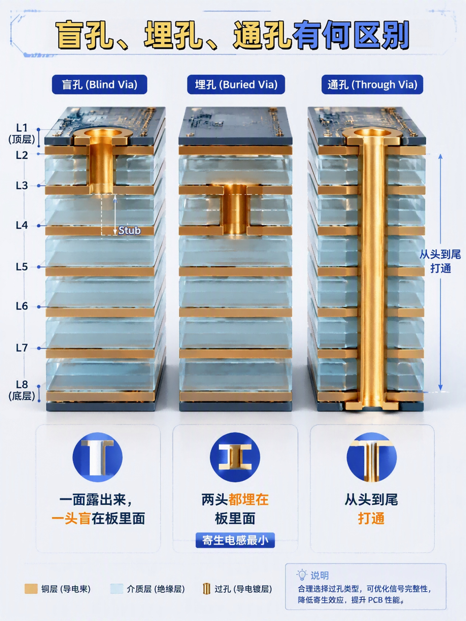
1. Blind Via
Drilled from the top or bottom surface of the PCB downwards using a laser, terminating at a specific inner layer without penetrating the entire board. Visually, the via opening is only visible on one side, not the other.
Example: Connections L1-L2 and L8-L7 in an 8-layer board.
Advantages: Short via depth, minimal stubs, low high-speed signal reflections; does not occupy BGA pads on the opposite side, making it the primary solution for BGA fan-out.
Process: Primarily uses laser drilling.
2. Buried Via
Completely hidden inside the PCB, located between inner core layers, with no visible openings on either the top or bottom surfaces.
Example: Connections L2-L3 and L4-L5 in an 8-layer board.
Advantages: Does not occupy any outer layer space, minimal parasitic inductance, excellent high-speed performance.
Process: Requires drilling and plating on inner core layers first, followed by lamination of multiple cores. After lamination, they cannot be observed externally.
3. Through Via
Drilled directly from the top layer through to the bottom layer, penetrating all layers of the PCB, with openings visible on both sides.
II. How to Distinguish HDI 1st/2nd/3rd Generation and Any-Layer?
Core Definition: HDI Generation = Number of outer layer build-up cycles (Lamination + Laser Drilling Blind Vias).
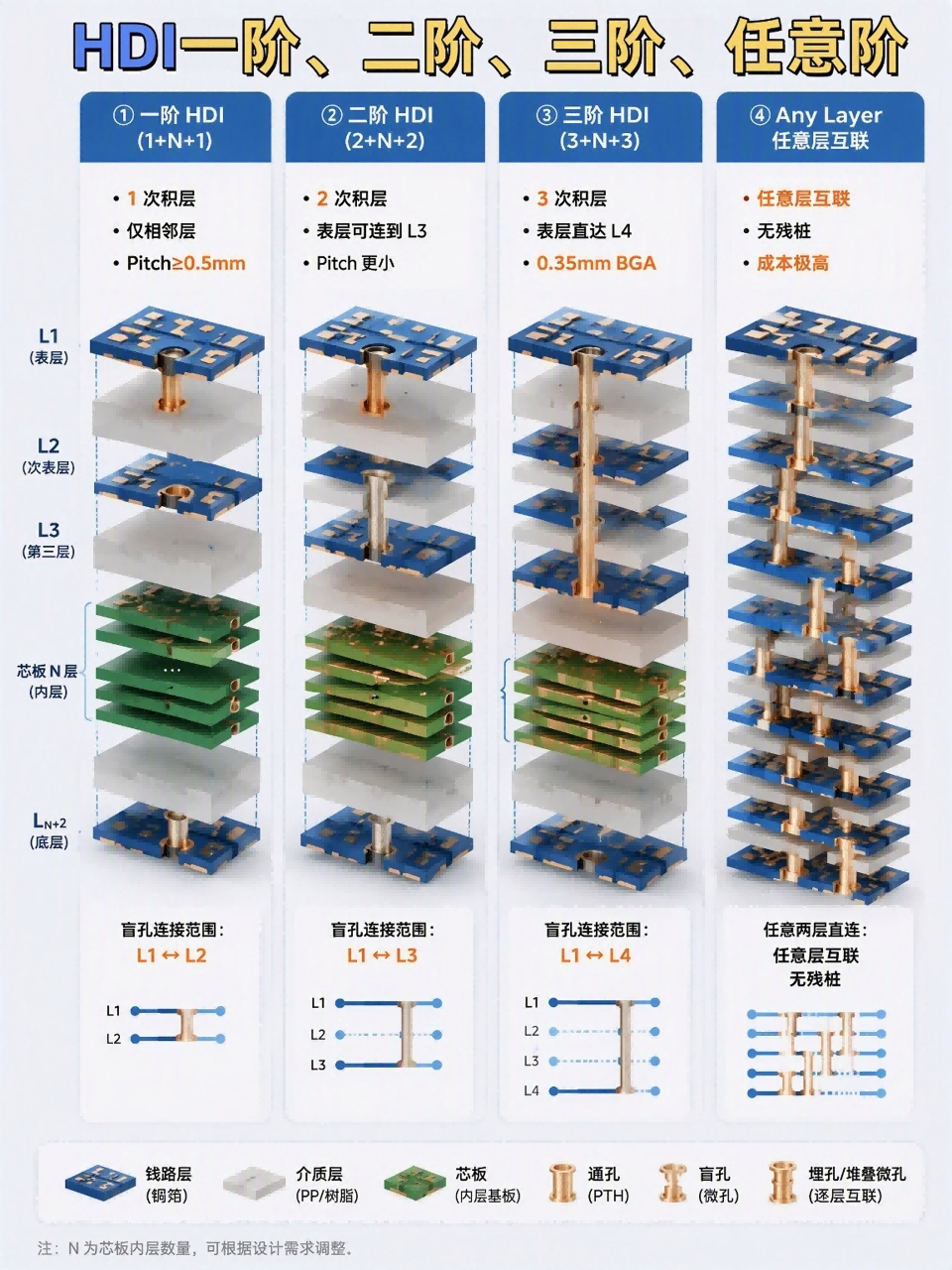
1. 1st-Generation HDI (Notation: 1+N+1)
Only one outer layer build-up cycle. Blind vias can only connect the outer layer to the immediately adjacent sub-outer layer (e.g., L1-L2, Ln-L(n-1)), but cannot span layers directly (e.g., L1-L3).
Structure: N core layers in the middle, with one dielectric layer laminated on top and bottom. Laser blind vias only penetrate the adjacent outer layers.
Application Scenarios: BGA Pitch ≥ 0.5mm.
Characteristics: Lowest cost, mature mass production process, widely used in consumer electronics and industrial control boards.
2. 2nd-Generation HDI (Notation: 2+N+2)
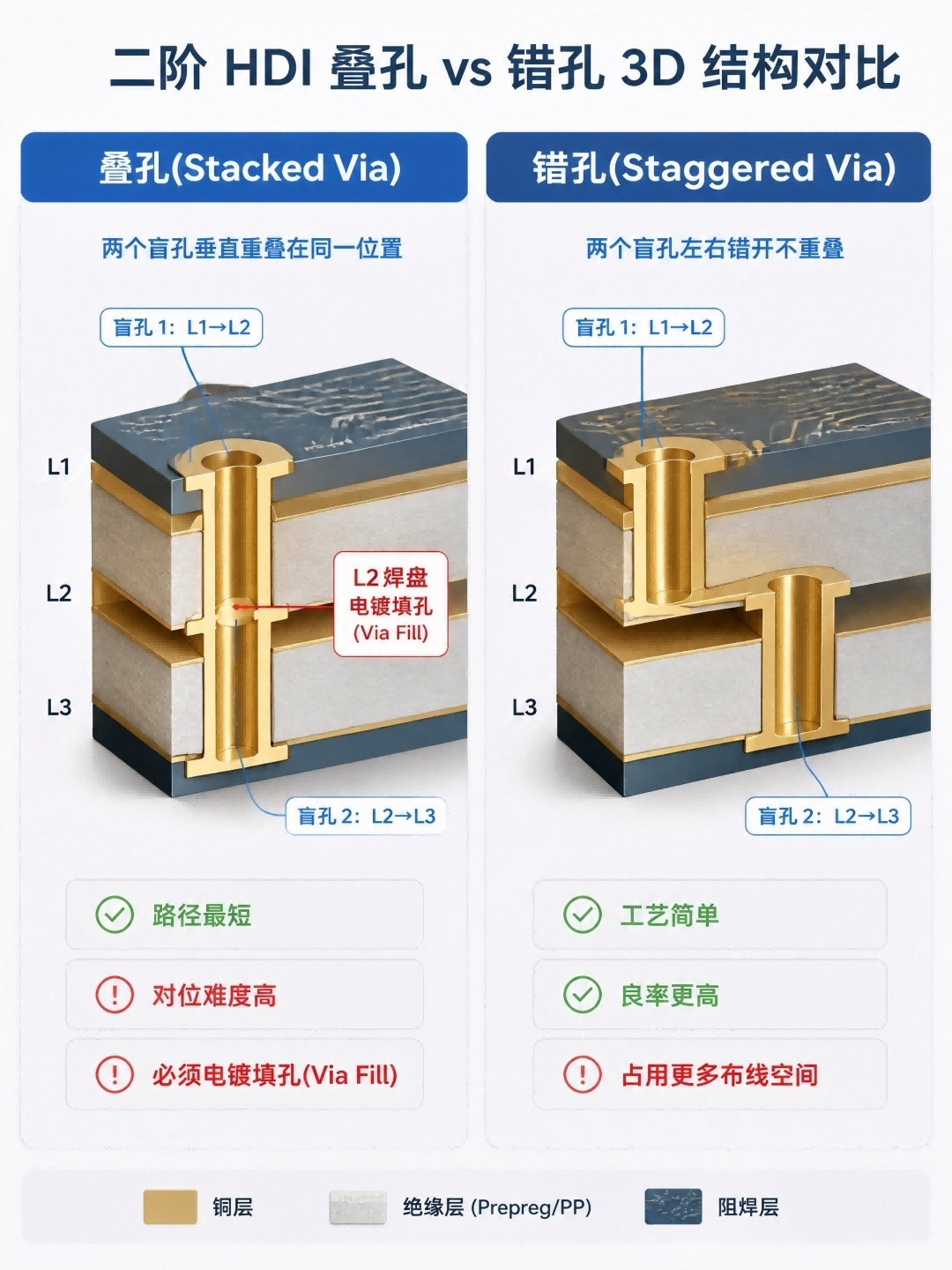
Two build-up cycles completed, allowing direct connection from the outer layer to Layer 3. The second generation has two structures, which are the most common pitfalls in engineering:
Stacked Via 2nd Gen: The L1-L2 blind via and the L2-L3 blind via are vertically aligned and stacked. The intermediate L2 pad requires electroplated hole filling. Shorter routing path, smaller stubs; however, higher alignment difficulty for the fab, slightly higher reliability risk, and more expensive.
Note: Stacked vias must explicitly require electroplated hole filling; resin plug holes alone are strictly prohibited.
Staggered Via 2nd Gen: The L1-L2 and L2-L3 blind vias are offset horizontally, not in the same vertical position. Simpler process, higher yield, lower cost than stacked vias; but occupies valuable routing channel space within the BGA area.
3. 3rd-Generation HDI (Notation: 3+N+3)
Three build-up cycles completed, allowing direct connection from the outer layer to Layer 4. Blind vias can stack up to three layers deep.
Application Scenarios: Ultra-small pitch BGAs (0.3mm, 0.35mm), AI computing chips, high-speed server motherboards.
Characteristics: Cost increases further, yield relatively decreases.
4. Any-Layer Interconnect (Any-Layer / Any Generation)
Abandons the traditional "large core N in the middle" architecture, adopting a layer-by-layer build-up approach. Laser blind vias can be drilled between any adjacent two layers, allowing direct interconnection between any two layers without needing through-via relays.
Advantages: Almost no stubs exist, reaching the ceiling of high-speed performance; perfectly suitable for ultra-dense BGA fan-outs below 0.3mm.
Characteristics: Extremely high price, mainly used in high-end smartphone motherboards, AI accelerator cards, etc.
III. Key Points for HDI PCB Design Selection and Pitfall Avoidance
1. Match BGA Pitch to HDI Process (Most Critical Selection Point)
Pitch ≥ 0.5mm: 1st-generation HDI is sufficient. Do not blindly upgrade to 2nd generation, adding unnecessary costs.
Pitch = 0.4mm: Prioritize 2nd-generation staggered vias for controlled costs; choose 2nd-generation stacked vias only when BGA routing space is extremely tight.
Pitch ≤ 0.35mm: Must use 3rd-generation or Any-Layer.
2. Principles for Choosing Between Stacked and Staggered Vias in 2nd Generation
Prioritizing cost control and production reliability → Choose 2nd-generation staggered vias.
Extremely tight BGA internal routing channels, insufficient space → Choose 2nd-generation stacked vias, and you must explicitly specify in the fabrication document: "Stacked vias require electroplated hole filling; resin plug holes are rejected."
3. Rules for Laser Blind Via Diameter and Pads
The minimum diameter for standard laser blind vias is 0.1mm (4mil).
Pad diameter must be ≥ 6mil larger than the via diameter, with a single-side annular width ≥ 3mil, to prevent pad breakage and open circuits.
Avoid drawing blind via pads as large as through-via pads, to save the limited space in the BGA area.
4. Focus on Stubs for High-Speed Signals
The shorter the blind via, the smaller the stub, the lower the signal reflection, and the better the high-speed performance.
Path length comparison: Stacked < Staggered; Any-Layer has almost no stubs, best suited for ultra-high-speed links like DDR5, PCIe 5.0, and high-speed SerDes.
5. Precautions for Using Buried Vias
Buried vias are drilled during the inner core stage and cannot be processed later by laser.
Buried vias are suitable for long-distance inner-layer interconnections; for high-speed BGA fan-outs, blind vias should be prioritized to reduce parasitic effects.
6. Cost and Lead Time Red Lines
For each increase in HDI generation, the PCB procurement price typically rises by 30%~50%, while lead times extend and yields decrease.
Selection Iron Law: Use 1st gen if possible instead of 2nd; use staggered if possible instead of stacked; use 2nd gen if possible instead of Any-Layer.
7. Clearly Specify Process Descriptions in Production Documents
Many engineers only output the stackup order but neglect HDI process descriptions. It is mandatory to clearly specify in the fabrication notes, e.g., "1+6+1 1st-Gen HDI", "2+6+2 2nd-Gen Staggered HDI". If not specified, the fab will process according to default methods, easily leading to process mismatches and batch scrapping.
The core of HDI selection is not "how many layers the board has," but balancing BGA pitch, fan-out channels, stub requirements, cost, and lead time. Clarifying the differences between blind, buried, and through vias, understanding the structural differences between 1st, 2nd, 3rd generations, and Any-Layer, and accurately expressing process requirements in fabrication documents are essential to avoid risks of changing stackups, re-fabricating, or scrapping later.
trending news
Contact Us