



Sorry, no sales person is available right now to take your call. Pls leave a message and we will reply to you via email as soon as possible.
Home/ PCB News/ Comprehensive Process Analysis of High-End PCB Embedded Resistor and Capacitor Mass Production
Comprehensive Process Analysis of High-End PCB Embedded Resistor and Capacitor Mass Production
2026-07-27
With the continuous iteration of high-end electronic devices such as 5G RF, millimeter-wave radar, high-speed servers, slim intelligent terminals, FPGA substrates, and SiP packaging, product miniaturization, high-speed signal transmission, and environmental reliability have become core design metrics. Embedded resistors (buried resistors) and embedded capacitors (buried capacitors) in PCBs represent a cutting-edge approach to passive component integration, offering a critical technological pathway to overcome traditional routing limitations and systematically optimize signal integrity (SI) and power delivery network (PDN) performance.
Compared with conventional surface-mount (SMT) discrete resistor and capacitor solutions, embedded passive components are directly integrated within the internal layers of the PCB substrate. This fundamentally avoids inherent drawbacks of surface-mounted components, such as large parasitic parameters, high board surface occupancy, susceptibility to environmental degradation, and poor resistance to vibration and thermal cycling. Owing to extremely low parasitic inductance, ultra-high routing density, and exceptional environmental reliability, this technology has become an essential core capability for mass production of high-end, high-density PCBs. Currently, several specialized PCB manufacturers in China have achieved scaled mass production of this process and accumulated extensive engineering and manufacturing experience.
Based on its proprietary buried resistor and capacitor processes, BaiNeng YunBan has systematically compiled a comprehensive overview covering technical definitions, key material characteristics, full-scale mass production workflows, critical process boundaries, core advantages, and typical application scenarios—balancing theoretical rigor with practical manufacturability. This resource is suitable for engineering R&D learning, production line process training, and industry-wide technical education.
I. Core Technical Definitions of Buried Resistors and Capacitors
1. Thin-Film Buried Resistors (R-Cu Process)
Thin-film buried resistors utilize specialized R-Cu resistive copper-clad laminate as the base material. Through precision processing, nano-scale NiCr (nickel-chromium) or TaN (tantalum nitride) resistive thin films are formed directly on the copper foil surface of the core laminate, enabling embedded resistor structures within inner PCB layers without requiring SMT placement.
This process delivers high resistance accuracy, excellent batch-to-batch consistency, and low temperature coefficients, precisely meeting the demands of high-precision circuit designs such as high-speed differential signal termination, impedance control, and current-limiting loops. Currently, mass-produced thin-film buried resistors typically cover a resistance range from 10Ω to 10kΩ, with standard sheet resistance values including 25Ω, 50Ω, and 100Ω—making them the preferred passive integration solution for high-frequency, high-speed PCB applications. For example, leading manufacturers like BaiNeng YunBan have stably achieved industry-leading planar resistor accuracy in mass production, satisfying the stringent requirements of high-end communication and computing products.
2. Planar Buried Capacitors (C-Ply Process)
Planar buried capacitors use high-dielectric-constant (High-Dk) embedded capacitor prepreg as the core material, forming a monolithic “sandwich” structure consisting of top copper foil + ultra-thin high-Dk dielectric layer + bottom copper foil. This creates a distributed array of embedded capacitors between the PCB’s power and ground planes.
This structure can replace large quantities of miniature MLCC chip capacitors (e.g., 0201, 0402), significantly freeing up board surface area for routing while dramatically enhancing high-frequency power decoupling performance, effectively suppressing high-frequency noise and improving overall PDN stability. Typical buried capacitor materials feature Dk values ranging from 16 to over 30, with dielectric thicknesses as thin as 8–20μm, yielding unit-area capacitance far exceeding that of traditional FR4 interlayer coupling. This process has already been integrated into the special-process capability portfolios of multiple professional manufacturers and is used in conjunction with buried resistors, embedded copper blocks, and stepped cavities to support advanced PCB designs.
II. Comparison of Core Materials and Process Characteristics
1. Buried Resistor Base Material: R-Cu Resistive Copper Laminate
Basic Structure: FR4 core laminate + conductive copper foil + NiCr/TaN nano-scale resistive thin film
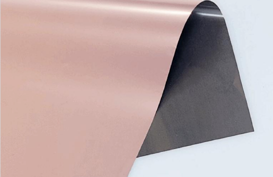
Key Process Characteristics: A dual-chemical selective etching system—comprising specialized resistive-film etchant and alkaline copper etchant—enables precise, selective removal of the resistive film and copper electrodes. Laser trimming supports fine resistance calibration, achieving mass-production resistance tolerances of ±1% to ±3%, meeting the precision demands of high-end circuits.
Thermal Stability: NiCr-based films typically achieve TCR (Temperature Coefficient of Resistance) within ±50ppm/℃, while TaN-based films can reach as low as ±25ppm/℃, ensuring stable resistance across wide temperature ranges.
2. Buried Capacitor Base Material: C-Ply Capacitor Prepreg
Basic Structure: Double-sided conductive copper foil + ultra-thin high-dielectric insulating layer
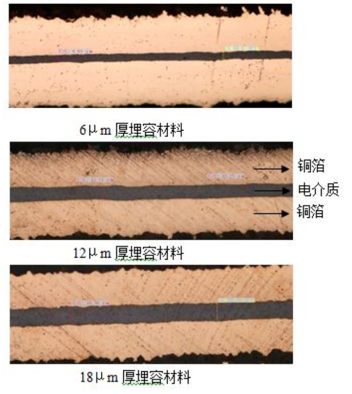
Key Process Characteristics: The process requires no special chemicals—standard acidic copper etchant suffices for electrode patterning, eliminating the need for laser trimming. Final capacitance is determined by two key parameters: electrode overlap area and dielectric thickness, both highly controllable, resulting in excellent production stability and yield.
Electrical Performance Advantages: Dielectric thickness uniformity directly impacts capacitance accuracy. High-quality buried capacitor materials maintain thickness tolerance within ±5%, corresponding to capacitance tolerance within ±10%.
III. Full Mass Production Workflow for Buried Resistors and Capacitors (Standardized Process)
(1) Precision Inner-Layer Process for Buried Resistors (High-Accuracy Core Step)
This step directly determines resistance accuracy and electrical reliability, representing the core of the entire process. Strict control must be maintained throughout regarding cleanroom conditions, chemical concentration and temperature, alignment accuracy, and operational protocols.
Process Flow:
Material Cutting (distinguish front/back of resistive film; prevent scratches or contamination) → Soft Surface Conditioning (light abrasion to remove copper oxide while preserving resistive film) → First Dry Film Lamination & Exposure (precisely mask resistor body, leaving etch window) → Specialized NiCr Resistive Film Etching (core step: accurately pattern nano-resistive film) → Film Stripping & Rinsing → Second Dry Film Lamination & Exposure (expose only electrode areas, protecting resistor body) → Alkaline Copper Etching (remove excess copper to form electrodes) → AOI Inspection (detect misalignment, residual copper, film damage) → Laser Trimming (fine-tune resistance value) → 100% Resistance Testing Before Lamination (reject out-of-spec panels)
Critical Process Parameter Control:
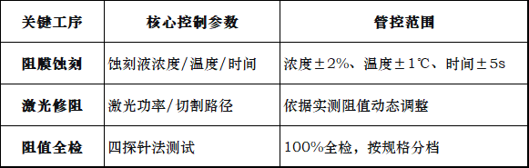
In actual mass production, leading manufacturers employ intelligent closed-loop control systems across all 36 precision chemical steps, effectively ensuring batch consistency and high yield for buried resistor processes.
(2) Inner-Layer Process for Buried Capacitors
Key controls focus on dielectric layer protection and electrode alignment accuracy to avoid lamination voids, capacitance drift, and dielectric damage.
Process Flow:
Material Cutting (handle gently to avoid bending, dents, or dielectric damage) → Mild Micro-Etching (clean copper surface without harming high-Dk dielectric) → Dry Film Lamination & Exposure (define capacitor electrode pattern) → Acidic Copper Etching → AOI Full Inspection (check for electrode misalignment, missing corners, residual copper) → 100% LCR Capacitance Testing Before Lamination
Critical Process Parameter Control:
(3) Unified Pre-Lamination Preparation for Inner Layers
After completing inner-layer processing and electrical testing for buried resistors and capacitors, unified pre-lamination treatment ensures interlayer bonding strength and prevents structural defects.
Low-Temperature Short-Duration Brown Oxidation (optimized parameters to avoid thermal damage to resistive film and high-Dk dielectric) → High-Precision Layer Stacking (drill paths avoid functional resistor/capacitor zones to prevent structural damage) → Vacuum Stepwise Lamination (low-pressure, slow degassing to eliminate voids, delamination, and dielectric shift)
Critical Lamination Parameters:
Ramp Rate: 1.5–3.0℃/min (segmented based on material Tg)
Peak Pressure: 250–350 psi (to prevent excessive dielectric deformation)
Vacuum Level: ≤20 mbar (ensures thorough degassing)
Dwell Time: ≥60 min (adjusted based on panel thickness and stackup)
For advanced HDI and hybrid buried-capacitor structures, interlayer alignment must be tightly controlled within ±25μm—a standard internal specification adopted by leading manufacturers to ensure precise electrode overlap area for capacitors.
(4) Standard Post-Lamination PCB Manufacturing Flow
Following lamination, boards enter standard high-end PCB back-end processes, with dedicated electrical retesting throughout to ensure final performance stability.
Mechanical Drilling → Plasma Desmear → Electroless Copper & Panel Plating → Outer Layer Imaging & Etching → AOI Inspection → Solder Mask Application & Curing → Laser Marking → Custom Surface Finish (ENIG, Immersion Silver, Hard Gold, etc.) → Final Buried R/C Parameter Retest → Profiling → FQC Full Outgoing Inspection
Special Considerations in Back-End Processes:
Drill holes must avoid functional buried R/C zones; drill toolpaths require safety margins (typically ≥0.3mm)
Outer layer alignment references must share the same coordinate system as inner buried R/C patterns to maintain stackup accuracy
Surface finish selection must account for potential impact on exposed resistor electrodes; nickel-gold plating may cause resistance drift
IV. Three Critical Process Boundaries in Mass Production (Keys to Yield)
Buried resistors and capacitors are irreversible embedded processes—once laminated, no repair or adjustment is possible. The following three items are absolute red lines in mass production; parameter excursions, skipped steps, or procedural violations are strictly prohibited.
1. Buried Resistor Red Line: Precision of Selective Resistive Film Etching
Selective etching of the resistive film is decisive for buried resistor success. Issues such as excessive undercutting, residual film, film breakage, or uneven etching directly cause resistance deviation or drift—and these defects cannot be corrected by laser trimming, necessitating full-panel scrapping.
Quantitative Control Standards:
Resistive film line width tolerance: ≤±10% (vs. design value)
Undercut: ≤20% of film thickness
Etch uniformity: ≤5% variation across panel
Chemical concentration drift: ≤±2% (monitored and replenished daily)
Mass production requires strict locking of chemical concentration, etch duration, and process temperature—implemented via real-time SPC (Statistical Process Control).
2. Buried Capacitor Red Line: Lamination Process Stability
Lamination directly determines buried capacitor reliability. Incomplete degassing causes internal voids, reducing dielectric strength and risking long-term delamination or breakdown. Stack misalignment alters effective electrode overlap area, leading to out-of-spec capacitance and failed high-frequency decoupling.
Quantitative Control Standards:
Stack alignment accuracy: ≤±50μm (X/Y directions)
Post-lamination dielectric thickness variation: ≤±10%
Void inspection: 100% X-ray scan; voids >0.5mm diameter = reject
Dielectric withstand test: per-batch sampling; breakdown voltage ≥2× rated operating voltage
3. Universal Principle: Electrical Testing Must Be Pre-Lamination
All electrical tests for buried resistor values and capacitor capacitance must be completed via 100% full inspection before lamination. Once sealed within layers, these components cannot be repaired, adjusted, or salvaged—any defective panel must be scrapped entirely. This principle is fundamental to yield management and cost control in mass production.
V. Core Technical Advantages of Buried Resistor and Capacitor Technology
1. Ultra-Compact Board Design, Enabling Miniaturization and Slim Form Factors
The embedded interlayer structure replaces hundreds to thousands of surface-mount passives per PCB, significantly increasing routing density, simplifying SMT assembly, and eliminating common SMT defects like cold solder joints, missing components, or part detachment. For example, in a typical FPGA substrate, adopting buried R/C technology reduces surface component count by 30–50%, freeing valuable space for routing and thermal management.
2. Ultra-Low Parasitics, Exceptional High-Frequency/High-Speed Performance
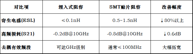
Embedded passives exhibit far lower parasitic ESL than conventional SMT parts (buried resistor ESL can reach ~0.1nH—~80% lower than 0603 chip resistors), effectively reducing high-frequency signal loss, suppressing crosstalk and resonance, and significantly enhancing SI and power decoupling efficiency. This makes the technology ideal for demanding applications like high-speed computing, RF, and millimeter-wave transmission.
Typical Electrical Comparison:
3. Hermetically Sealed Interlayer Structure, Exceptional Environmental Reliability
Functional R/C structures are fully encapsulated within the PCB substrate, isolated from air, moisture, dust, and corrosive environments. They exhibit outstanding performance in thermal cycling (-65℃ to +125℃ / 1000 cycles), mechanical vibration (compliant with MIL-STD-202G), and oxidation resistance—ensuring long-term stability in industrial control, automotive electronics, and precision medical equipment.
4. Standardized Process, Suitable for High-Volume Manufacturing
Built on mature standardized materials, fixed process parameters, and pre-lamination full inspection, the technology delivers excellent repeatability and batch consistency (CPK ≥1.33), enabling effective yield control and fully meeting the high-reliability, high-volume delivery demands of premium PCBs.
VI. Mainstream Commercial Applications
This technology targets high-end, high-density PCBs and is widely deployed across precision, high-speed, and high-reliability electronics:
Communications & Networking:
5G/6G RF front-end modules (impedance matching for PA, LNA, filters)
Millimeter-wave radar boards (automotive ADAS, traffic monitoring)
High-speed optical transceivers (400G/800G)
Computing & Storage:
High-speed server motherboards & backplanes (CPU PDN decoupling)
FPGA core substrates (integrated passives in BGA fanout zones)
High-performance computing (HPC) motherboards
Packaging & Modules:
SiP (System-in-Package) substrates
RF front-end module (FEM) substrates
Power management unit (PMU) substrates
Industrial & Automotive:
High-end industrial control motherboards
Automotive domain controllers & smart cockpit motherboards
Precision medical electronics (ultrasound, CT, etc.)
Typical Integration Benefits: In a high-speed server power module, adopting buried capacitors reduced PDN impedance by ~40% in the 100MHz–1GHz band, improved power supply ripple rejection ratio (PSRR) by ~15dB, and eliminated ~2000 surface-mount capacitors—reducing SMT cycle time by ~30%.
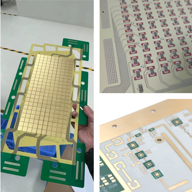
In these high-end applications, specialized PCB manufacturers with buried R/C capabilities play a pivotal role. For instance, BaiNeng YunBan has delivered scaled mass production for automotive millimeter-wave radar, high-speed server power modules, and FPGA core substrates, covering high-precision multilayer, HDI, and high-frequency/high-speed PCBs across its portfolio.
BaiNeng YunBan Buried Resistor, Capacitor, and Chip Product Showcase
VII. Conclusion
Embedded resistor and capacitor technology is not a niche customization—it is a core competitive capability for today’s high-end, high-density PCBs and a foundational enabler of miniaturization, high-speed performance, and high reliability in electronic systems.
Successful mass production hinges on three pillars:
① Precise mastery of R-Cu resistive film and C-Ply high-Dk dielectric material properties and process windows;
② Strict adherence to the three red lines: selective resistive film etching, lamination stability, and pre-lamination full electrical testing;
③ Systematic establishment of end-to-end quality control—from material selection and process parameters to electrical verification.
As 5G Advanced, AI compute clusters, and L3+ autonomous driving accelerate, demand for buried R/C in high-frequency/high-speed PCBs is shifting from “optional” to “mandatory.” Mastering this core know-how and building a complete closed-loop capability—from design simulation to mass production control—will be key for high-end PCB manufacturers to establish technological moats in the next phase of industry competition.
Through standardized processes and rigorous quality control, embedded passive technology will continue to provide robust foundational support for performance upgrades and reliability enhancement in high-end electronics, driving new heights in system integration density and performance density.
trending news
Contact Us