



Sorry, no sales person is available right now to take your call. Pls leave a message and we will reply to you via email as soon as possible.
Home/ PCB News/ Ceramic Substrate Selection FAQ: A Comprehensive Guide Covering Material, Process, and Cost
Ceramic Substrate Selection FAQ: A Comprehensive Guide Covering Material, Process, and Cost
2026-07-22
Ceramic substrates are critical carrier materials for power semiconductors, optoelectronic devices, and high-frequency components. The selection of substrate material and metallization process directly affects thermal dissipation efficiency, thermal cycling reliability, and current-carrying capacity, profoundly influencing project costs and mass production yield. In practice, cases of thermal runaway due to material mismatch, delamination or cracking caused by process misjudgment, and budget overruns from inaccurate cost estimation are frequently encountered.
This article systematically organizes industry-standard selection logic, typical application scenarios, and key pitfalls to avoid—covering consumer electronics, industrial power supplies, new energy vehicles, and rail transit—through an engineer-focused FAQ format across three dimensions: material properties, process compatibility, and cost control.
I. Materials: Selection Logic for Three Mainstream Ceramic Substrates
Currently, the most widely used ceramic substrates in power packaging mass production are aluminum oxide (Al₂O₃), aluminum nitride (AlN), and silicon nitride (Si₃N₄). These three differ significantly in performance, reliability, and cost. Precisely matching application requirements is the primary principle of material selection.
Q1: Core Parameter Comparison and Selection Guidelines for the Three Ceramic Materials
Under room temperature conditions (25°C), key performance characteristics and cost positioning are as follows:
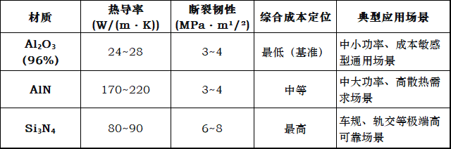
Selection Mnemonic: Choose Al₂O₃ for standard power applications where cost is prioritized; select AlN for high heat flux density scenarios where thermal management is critical; opt for Si₃N₄ when operating under severe thermal cycling conditions requiring long-term durability.
Q2: AlN offers far superior thermal conductivity compared to Al₂O₃—why does Al₂O₃ still dominate the market?
Performance beyond necessity isn't required—cost and process maturity dictate mass production success.
Sufficient Performance: In low-to-medium power applications, heat flux density typically remains below 50 W/cm². Al₂O₃’s thermal conductivity of 24–28 W/(m·K) is fully adequate for power modules, standard LEDs, and consumer power devices, presenting no thermal bottleneck.
Significant Cost Advantage: Al₂O₃ substrates cost approximately one-third to one-fifth of AlN. Moreover, Al₂O₃ is best suited for DBC processing, offering mature, stable yields and high tolerance—making its overall economics vastly superior to AlN in mass production.
Clear Upgrade Threshold: Switching to AlN is only justified when heat flux density consistently exceeds 50 W/cm² or when thermal issues become the primary cause of system failure.
Q3: Si₃N₄ is the most expensive—when is it truly indispensable?
Although Si₃N₄ lacks cost-effectiveness, it is irreplaceable in applications demanding ultra-high reliability. Its fracture toughness is twice that of Al₂O₃ or AlN, enabling it to withstand frequent thermal shocks between -40°C and 150°C, effectively preventing substrate cracking and copper layer delamination.
Mandatory Use Cases:
Automotive-grade SiC power modules (for motor control and traction inverters)
Rail transit traction converters
Other equipment requiring stringent thermal cycling lifetime validation
In these scenarios, conventional ceramic substrates fail reliability validation, making Si₃N₄ the only viable mature option.
Q4: Beryllium oxide (BeO) exhibits excellent thermal conductivity—why has the industry abandoned it?
BeO achieves thermal conductivity of 250–300 W/(m·K), surpassing AlN. However, its fatal flaw lies in the high toxicity of beryllium and its compounds. Throughout its lifecycle—including cutting, grinding, and waste handling—beryllium-containing dust poses irreversible health risks to personnel, violating modern industrial safety and environmental standards.
Today, BeO is retained only in extremely limited military and aerospace custom applications.Its use is strictly prohibited in civilian and industrial projects..
II. Processes: Precise Matching of DBC / AMB / DPC Metallization Technologies
Once the substrate material is selected, the metallization process determines circuit precision, bond strength, current-carrying capacity, and long-term reliability. The three mainstream mass-production processes—DBC, AMB, and DPC—have clearly defined application boundaries and cannot be simply interchanged.
Q5: Core Parameters and Selection Criteria for DBC, AMB, and DPC
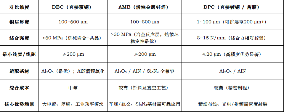
Selection Mnemonic: For thick copper and high current, choose between DBC and AMB based on needs; Si₃N₄ must be paired with AMB; for line widths ≤50 μm, only DPC is suitable.
Q6: Is AMB the only viable metallization process for Si₃N₄ substrates?
Yes—AMB is currently the only mature, mass-producible metallization solution for Si₃N₄.
DBC relies on Cu-O eutectic reactions, which only work with oxide ceramics. Si₃N₄ surfaces cannot form an effective eutectic interface, rendering DBC technically unfeasible.
DPC exhibits relatively low bond strength and is prone to delamination and copper peeling under prolonged thermal cycling, failing to meet automotive-grade reliability requirements.
AMB uses Ti from Ag-Cu-Ti active brazing filler to react with Si₃N₄, forming a stable TiN interfacial layer that enables high-strength metallurgical bonding. Its thermal shock resistance and fatigue endurance have been thoroughly validated.
Q7: Can thick-copper DPC replace DBC? What is their true relationship?
With process advancements, thick-copper DPC (≥200 μm) can now cover some low-to-medium power DBC applications. However, the two are fundamentally complementary, not substitutable.
DPC’s Core Limitation: Ultra-fine circuits (≤20 μm) make it ideal for optoelectronics, RF, and high-density integration. However, its interfacial bond strength and long-term high-temperature stability remain inferior to DBC, limiting its ultimate current capacity and thermal cycling endurance.
DBC’s Core Strength: High bond strength, high current capacity, and long-term operational stability—but incapable of fine-feature processing.
Selection Principle: Prioritize DPC for precision; choose DBC for reliability and high current. Thick-copper DPC serves only as a compromise for moderate power with fine features and is unsuitable for extreme operating conditions.
III. Cost: Balancing Performance and Budget
Ceramic substrate cost is determined by three key factors: base material, metallization process, and production volume. Understanding cost structure enables precise selection that avoids over-engineering and budget overruns.
Q8: Cost Gradient Among the Three Base Materials and Root Causes of Premium Pricing
Using 96% Al₂O₃ as the baseline (unit price = 1), relative pricing and reasons for premium are as follows:
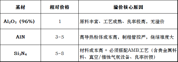
Note especially: The high cost of Si₃N₄ substrates stems not solely from the base material—specialized AMB equipment, consumables, and yield loss are the primary drivers of its premium pricing.
Q9: How to Achieve Optimal Performance-Cost Trade-offs in Mass Production Selection?
For non-extreme operating conditions, three proven cost-reduction strategies are recommended:
AlN + Pre-oxidized DBC (as an alternative to AlN+AMB)
In industrial high-thermal-conductivity applications that don’t require automotive-grade reliability, pre-oxidizing AlN allows compatibility with standard DBC processing—eliminating the need for expensive AMB brazing alloys and vacuum processing while meeting typical high-heat-dissipation requirements.
Thick-copper Al₂O₃-DBC (as an alternative to standard AlN solutions)
Under moderate heat flux, increasing the copper thickness on Al₂O₃ substrates from 300 μm to 500 μm significantly enhances lateral heat spreading and current capacity, compensating for the lower thermal conductivity of the base material—at a total cost far below switching to AlN.
Thick-copper DPC (as an alternative to secondary DBC processing)
In applications requiring fine circuits and moderate power, using thick-copper DPC (≥200 μm) eliminates the need for secondary patterning of DBC substrates, streamlining the process and balancing precision with cost.
Q10: Cost Differences Between Small-Batch Prototyping and Mass Production—and Cost-Saving Tips
In ceramic substrate cost structures, non-recurring engineering (NRE) fees account for a very high proportion, making batch size significantly impact per-unit pricing:
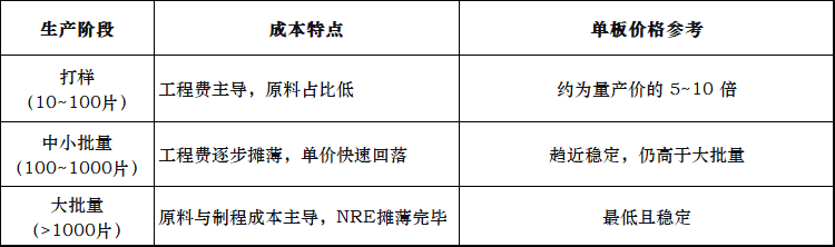
Cost-Saving Advice: During prototyping, don’t overly focus on per-unit price. Instead, prioritize suppliers offering a “prototype NRE fee credit toward future mass production orders” policy—effectively amortizing upfront R&D investment and avoiding wasted capital.
IV. Baineng Yunban Ceramic Substrate Capabilities Quick Reference
Baineng Yunban provides one-stop ceramic substrate services covering all materials, all processes, and all stages (prototyping → pilot run → mass production), rapidly matching diverse needs across consumer, industrial, new energy, and optoelectronic/RF sectors:
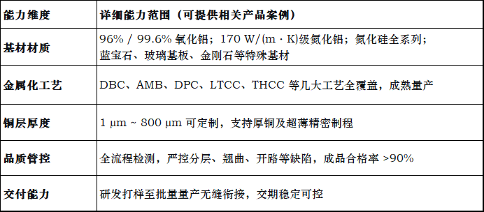
If you have specific project selection, process evaluation, or quotation needs, please provide your design parameters and operating conditions. We guarantee to deliver a customized process solution and accurate quotation within the same day, accelerating your project implementation.
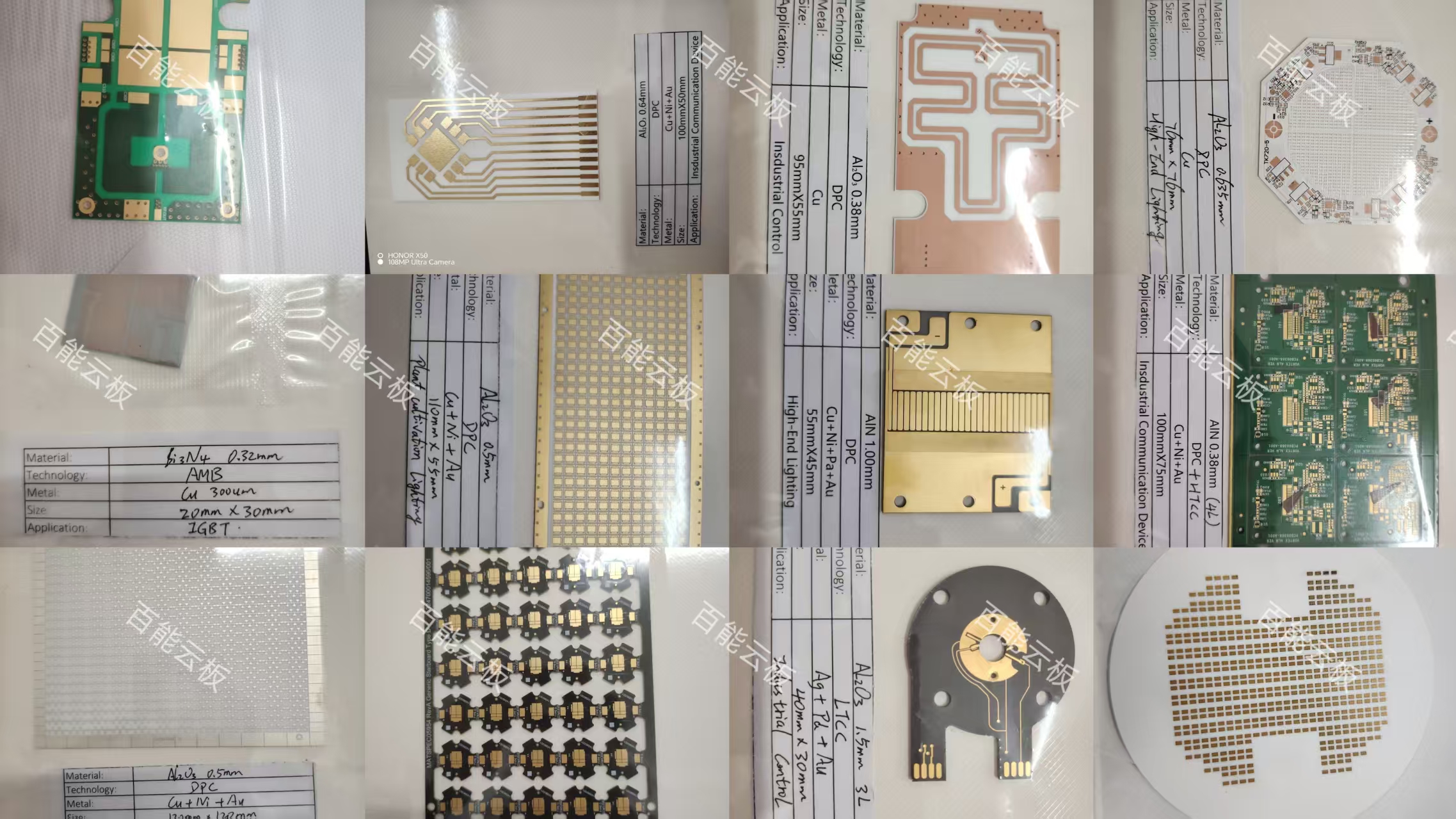
Selected Ceramic Substrate Products from Baineng Yunban
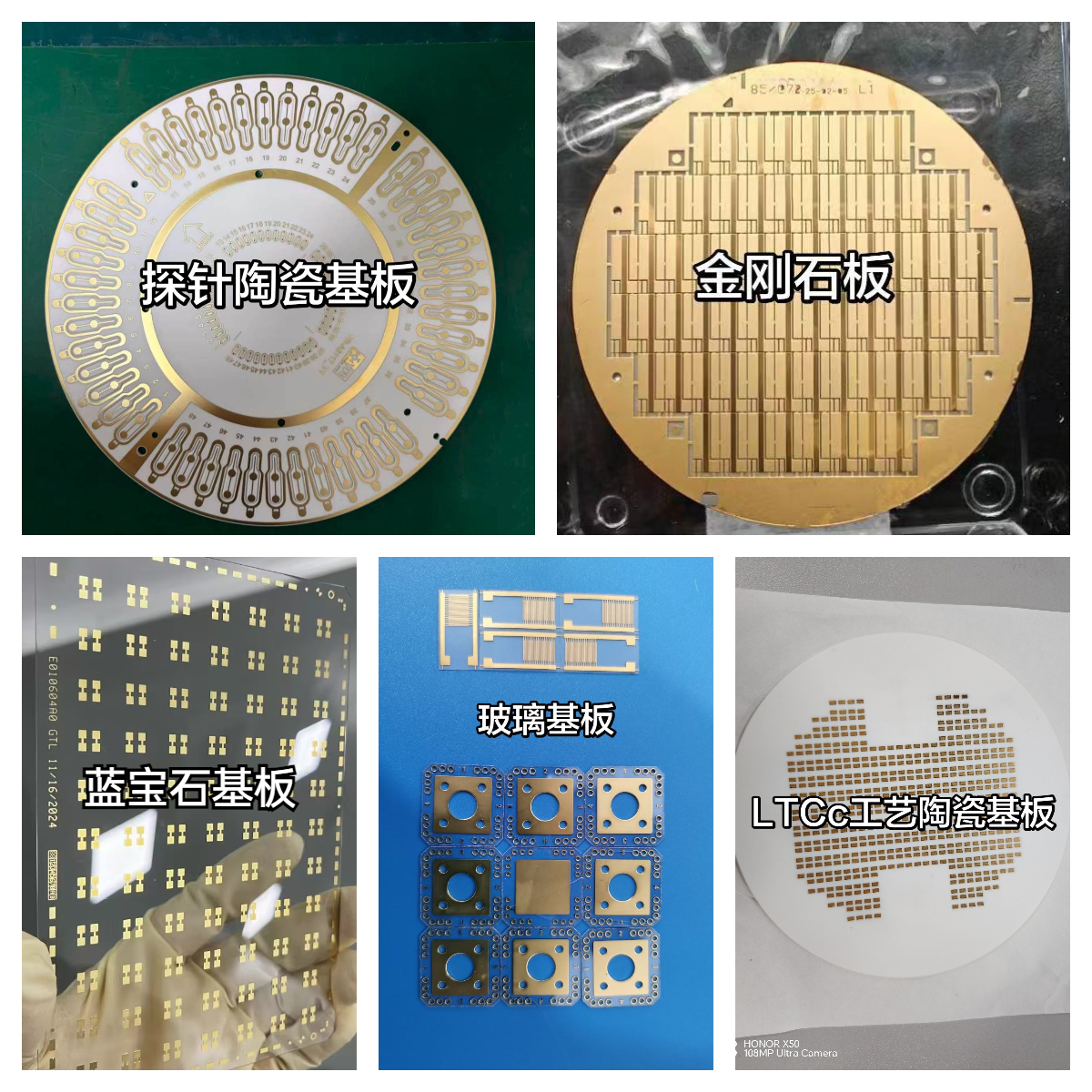
Selected Special Ceramic Products from Baineng Yunban
trending news
Contact Us