



Sorry, no sales person is available right now to take your call. Pls leave a message and we will reply to you via email as soon as possible.
Home/ PCB News/ Selection of PCB Gold Finger Edge Copper Exposure vs. Non-Exposure Processes for Optical Modules and Corrosion Prevention Solutions for Exposed Copper
Selection of PCB Gold Finger Edge Copper Exposure vs. Non-Exposure Processes for Optical Modules and Corrosion Prevention Solutions for Exposed Copper
2026-07-21
The gold fingers on optical module PCBs serve as the core interface for physical mating and electrical interconnection between the optical module and host devices such as switches and servers, responsible for delivering power, grounding, control signals, and high-speed data transmission. Their design, process selection, and material configuration always revolve around two primary objectives: high-speed signal integrity and long-term hot-plug reliability. In the development of ultra-high-speed optical module PCBs (400G/800G/1.6T), two process approaches—exposed copper edges versus non-exposed copper edges—significantly and differentially impact high-frequency electrical performance, manufacturing yield, and in-service reliability. Due to stringent impedance continuity requirements, many high-speed projects are compelled to adopt the exposed copper edge structure, which inherently carries the risk of oxidation and corrosion at the copper cross-section. Benengyun Board systematically compares the technical characteristics and engineering trade-offs of these two process schemes and proposes a comprehensive corrosion mitigation strategy specifically for the exposed copper edge architecture, aiming to provide reference guidance for hardware design and process selection of high-speed optical module PCBs.
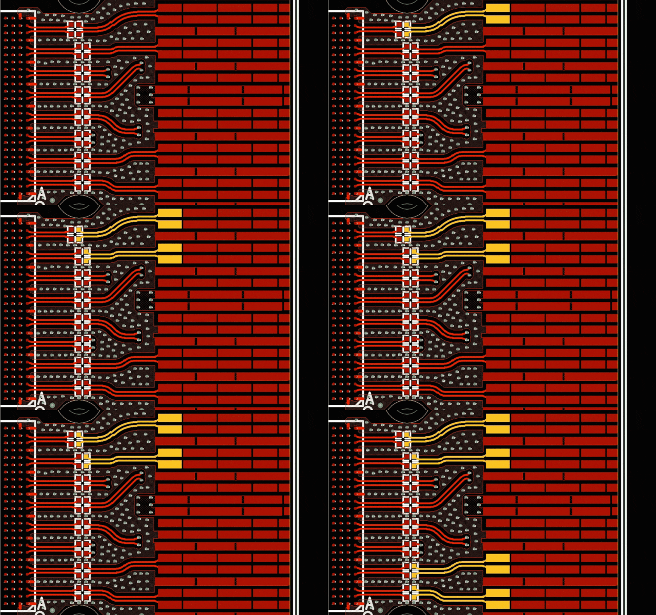
1. Comparison of Process Characteristics: Exposed vs. Non-Exposed Copper Edges
1.1 Exposed Copper Edges (Bare Copper Cross-Section)
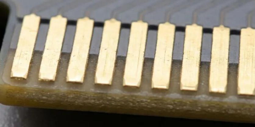
Exposed copper edges refer to a condition where, after PCB routing or punching, the copper foil cross-section at the outer side of the gold fingers is directly exposed to the external environment without solder mask or metal plating coverage.
Advantages
Better high-speed signal integrity: Optical modules operating at 400G, 800G, and beyond are extremely sensitive to impedance consistency. The clean, regular cross-section of exposed copper avoids impedance discontinuities caused by solder mask or plating, effectively reducing high-speed signal reflections and minimizing signal distortion.
Simpler process and cost-effective: Forming requires only standard routing or punching, with no additional edge protection steps. This shortens the process flow, improves mass production efficiency, and helps control manufacturing costs.
Potential Risks
Significant oxidation and corrosion risk: The bare copper cross-section is directly exposed to air, moisture, and environmental contaminants, making it prone to oxidation and even copper rust over time, leading to continuously increasing contact resistance and potential communication errors.
Higher risk of gold finger delamination: During repeated hot-plugging, lateral shear stress acts on the gold finger edges. The exposed copper cross-section represents a weak interface between plating and substrate, making it susceptible to gold layer peeling, lifting, or even flaking after multiple insertions.
Risk of copper debris causing short circuits: Copper burrs or fine particles generated during forming can migrate to adjacent pins under insertion pressure, potentially causing micro-shorts between channels.
1.2 Non-Exposed Copper Edges (Edge Protection Schemes)
Non-exposed copper edges are typically achieved via two methods: applying solder mask (green oil) over the edge or fully encapsulating the copper cross-section with nickel-gold plating, thereby isolating the copper from the external environment.
Advantages
Long-term oxidation and corrosion resistance: The copper cross-section is completely sealed by solder mask or nickel-gold plating, blocking moisture and air, thus fundamentally preventing edge oxidation, discoloration, and rust.
Enhanced hot-plug durability and extended service life: The protective layer (gold or solder mask) acts as a buffer against lateral stresses during insertion/extraction, significantly reducing the likelihood of edge delamination, peeling, or other failures—ideal for telecom-grade and data center equipment requiring frequent hot-plugging.
Superior appearance stability: Strong resistance to environmental aging meets the stringent appearance and reliability standards of high-end communication equipment.
Disadvantages and Design Challenges
Increased difficulty in high-speed impedance design: In high-bandwidth signaling scenarios like PAM4, the edge-encapsulating dielectric (solder mask has a different dielectric constant than the PCB substrate) introduces local impedance perturbations, necessitating precise electromagnetic simulation for accurate impedance modeling and compensation.
Higher process complexity and cost: Edge plating is a non-standard PCB process requiring specialized steps, resulting in longer production cycles, narrow process windows, greater yield control challenges, and significantly higher overall costs. PCB manufacturers with specialized capabilities—such as Benengyun Board—have accumulated extensive experience in high-precision, high-layer-count, and special-process PCBs, offering technical support and mass-production feasibility assessments for unconventional processes like edge plating.
2. Comprehensive Corrosion Mitigation Measures for Exposed Copper Edge Structures
In many high-speed optical module projects, hardware design is constrained by extreme signal integrity requirements, making edge plating or solder mask coverage impractical, thus necessitating the use of exposed copper edges. In such cases, integrated improvements must be implemented across multiple dimensions—including PCB process control, plating optimization, system-level protection, and storage/logistics—to maximize corrosion resistance while maintaining electrical performance.
2.1 Source-Level PCB Manufacturing Process Optimization
Routing Process Control
Diamond-coated milling cutters should be prioritized for shaping the gold finger area, with optimized spindle speed and feed rates to minimize burrs, delamination, and micro-cracks on the copper edge—rough surfaces more readily absorb moisture and accelerate corrosion. Post-forming, plasma cleaning or precision soft-brush deburring should be added to remove microscopic copper debris and sharp edges. Additionally, cooling media used during routing must be strictly controlled to prevent acidic cutting fluid residue on the edge, which could cause pre-corrosion of the copper substrate. At the mass production level, PCB manufacturers with full digital production capabilities can use intelligent production management systems to monitor routing parameters and quality data in real time, ensuring process consistency.
Standardized Cleaning and Drying Procedures
After forming and deburring, a complete sequence of degreasing, micro-etching, and multi-stage high-pressure rinsing must be performed to thoroughly remove organic contaminants and corrosive ions (e.g., chloride) from the edge. Immediately after cleaning, rapid hot-air drying must be applied; wet boards must never be left idle for extended periods, as continuous water films can trigger electrochemical corrosion.
Temporary Edge Protection Scheme
If extended bare-board storage or handling is required, a nano-scale water-soluble copper antioxidant can be applied to form an ultra-thin organic protective film on the edge.
Critical Constraint: The protective film thickness must be tightly controlled to avoid disturbing the electromagnetic field distribution at the gold finger edge or degrading impedance characteristics. Additionally, hot-plug validation must confirm that the coating does not transfer to the contact area during repeated insertions, causing poor contact. This solution is suitable only for temporary protection during storage and transportation and cannot meet long-term in-service corrosion resistance requirements.
2.2 Plating and Substrate Material Optimization
Optimized Nickel-Gold Plating System
Slightly thickening the barrier nickel layer helps block lateral penetration of moisture and corrosive agents along the plating interface, delaying corrosion spread from the edge toward the active contact zone. Low-porosity hard gold plating is preferred to reduce the risk of corrosive media penetrating through micro-pores in the gold layer to reach the underlying copper. Additionally, the transition zone at the gold edge should be optimized to minimize abrupt step changes. In practice, mature hard gold plating solutions for gold fingers are available, achieving gold thicknesses up to 50μm, eliminating lead residues between segmented fingers, and enabling minimum finger spacing as tight as 5 mil. Combined ENIG (Electroless Nickel Immersion Gold) and gold finger (30μ") processes also offer excellent corrosion resistance and conductivity, ensuring stable transmission of critical signals.
Copper Foil Selection Control
Low-roughness electrodeposited copper foil is recommended for the gold finger area. High-roughness copper foil has dense micro-pores on its cross-section that easily trap moisture and contaminants, significantly accelerating oxidation and corrosion.
2.3 System-Level Protection at the Host Device Level
Operating Environment Control
Data centers and telecom rooms should maintain stable temperature and humidity, avoiding prolonged high-humidity or condensation conditions. Additionally, concentrations of corrosive gases such as hydrogen sulfide and nitrogen oxides should be controlled to reduce atmospheric corrosion rates.
Collaborative Structural and Airflow Design
Host connectors can incorporate dust shields to reduce direct airflow onto the gold finger edges, minimizing continuous deposition of dust and corrosive agents. Overall system airflow should be designed to prevent condensation from directly contacting the gold finger area.
Packaging and Storage Standards
Bare PCBs and semi-finished optical modules should be vacuum-sealed in moisture-barrier bags with desiccants. Long-term inventory items can use VCI (Vapor Corrosion Inhibitor) packaging to suppress copper oxidation. Additionally, exposure time of bare boards to ambient air must be strictly limited.
2.4 Alternative Fundamental Solutions (Reliability-Priority Scenarios)
When long-term reliability outweighs ultimate signal integrity requirements, the exposed copper edge architecture should be re-evaluated in favor of the following protective schemes:
Edge Plating Process: Fully encapsulate the routed edge cross-section with nickel-gold plating to hermetically seal the copper substrate, eliminating oxidation risk at the source. Prior to implementation, signal integrity simulations must assess the impact of edge impedance variations on PAM4 high-speed signals.
Localized Solder Mask on Gold Finger Edges: Apply solder mask to the edge cross-section without interfering with the active mating contact area. Suitable for optical modules with relatively lower data rates and wider impedance tolerance.
3. Common Engineering Questions and Solutions (FAQ)
Addressing frequent points of contention regarding process selection and corrosion mitigation in practical implementation, the following Q&A provides quick reference for R&D and process engineers:
Q1: Does the exposed copper edge scheme inevitably lead to corrosion failure? What are the evaluation criteria?
A: Not necessarily. Corrosion failure depends on whether a continuous "water film + oxidant (e.g., oxygen, sulfides)" environment exists on the copper edge. In clean, temperature- and humidity-controlled data center environments, the corrosion rate of exposed copper edges is extremely low and can remain within acceptable contact reliability limits throughout the product’s design life. Evaluation typically relies on 85°C/85% RH damp heat testing or Mixed Flowing Gas (MFG) testing for accelerated validation, using contact resistance increase (e.g., >10–20% change) as the failure criterion—not merely visual discoloration.
Q2: Why not apply standard conformal coating directly to the exposed copper edge?
A: Standard conformal coatings are relatively thick (typically >25μm) and have a dielectric constant significantly different from the PCB substrate, causing capacitive impedance discontinuities at the gold finger edge that unacceptably degrade eye diagram margin for 56G/112G PAM4 signals. Moreover, the coating can peel off under insertion pressure, and the debris may exacerbate contact contamination. Therefore, nano-scale antioxidant films with tightly controlled thickness—or intrinsic corrosion resistance through plating and material improvements—are preferred over conventional coatings.
Q3: What is the actual impact of edge plating on high-speed signals, and what should be noted during simulation?
A: Edge plating effectively adds a localized conductive boundary at the gold finger edge, altering the high-frequency electromagnetic field distribution and typically causing a low-impedance dip (approximately 2–5Ω variation) on the impedance profile, depending on plating thickness and edge geometry. Simulation must employ a 3D full-wave electromagnetic solver (e.g., HFSS, CST), incorporating the plating’s conductivity, surface roughness, and the PCB stack-up’s dissipation factor (Df). 2D field solvers cannot accurately capture this edge effect and may yield significant discrepancies between simulation and measurement.
Q4: If cost constraints mandate exposed copper edges in mass production, how can incoming PCB batches with high corrosion risk be identified?
A: Two additional incoming inspection criteria are recommended:
① Cross-section microstructure inspection (using SEM to assess shear bands and micro-crack density on the copper edge);
② Ionic contamination testing (per IPC-TM-650, focusing on chloride and sulfate residues, with thresholds recommended at ≤0.8μg/cm² and ≤1.2μg/cm², respectively). These metrics effectively screen out high-risk batches caused by improper routing parameters or inadequate cleaning, preventing defective PCBs from entering assembly. PCB manufacturers with comprehensive testing capabilities typically equip copper thickness gauges and AOI systems to perform batch screening of these parameters prior to shipment.
Q5: If blackening is observed on the gold finger edge after deployment, must the module be scrapped?
A: A tiered assessment is required. If discoloration is confined to the non-contact edge area and contact resistance increase remains within design margin (typically <5%), localized cleaning with anhydrous ethanol or a dedicated gold finger cleaner may allow continued use. However, if blackening has migrated into the effective contact zone (i.e., the area actually contacted by the connector spring fingers) or contact resistance shows abrupt increases, it indicates penetration of the nickel/gold layers and irreversible copper corrosion. In this case, the module must be replaced to avoid bit error rate (BER) spikes or system-level link failures.
Q6: How to decide between exposed and non-exposed copper edges during PCB design?
A: Use the following decision flow:
① For single-lane rates ≤ 28G NRZ (corresponding to 100G and below optical modules), prioritize non-exposed copper edges (solder mask or edge plating), as reliability benefits are clear and impedance margin is sufficient;
② For single-lane rates ≥ 56G PAM4 (400G and above), further evaluate: if thermal conditions are favorable and hot-plug cycles ≤ 200 (e.g., fixed telecom ports), exposed copper edges may be acceptable;
For high-cycle applications like data center AOCs or active optical cables, upgrade to edge plating with upfront simulation-based compensation to balance reliability and signal integrity.
For high-complexity, high-precision optical module PCB customization, early process feasibility assessment and risk prediction from a full-service PCB manufacturer are recommended.
Through the systematic process selection, end-to-end corrosion mitigation strategies, and clarification of common concerns outlined above, designers can effectively identify and manage corrosion risks associated with exposed copper edge structures while meeting ultra-high-speed signal integrity requirements, thereby ensuring reliable design and long-term stable operation of high-speed optical module products.
trending news
Contact Us