



Sorry, no sales person is available right now to take your call. Pls leave a message and we will reply to you via email as soon as possible.
Home/ PCB News/ A Comprehensive Guide to Understanding PCB Impedance Control (In-Depth Article)
A Comprehensive Guide to Understanding PCB Impedance Control (In-Depth Article)
2026-07-20
In traditional low-speed PCB design, traces only needed to ensure electrical connectivity and current-carrying capacity; impedance parameters were not a primary concern. However, as electronic devices evolve toward higher speeds, higher frequencies, and miniaturization, high-speed interfaces such as DDR, PCIe, HDMI, and USB 3.0 have become standard. With significant increases in signal edge rates and operating frequencies, conventional low-speed design methodologies are no longer sufficient for high-speed circuit applications.
In high-speed signal scenarios, the precision and continuity of PCB trace characteristic impedance directly determine system signal integrity (SI), operational stability, and transmission reliability. Impedance control is central to modern high-speed PCB design and precision manufacturing, and it is the key method for addressing SI issues such as signal reflection, crosstalk, waveform distortion, and timing anomalies.
Engineering Pain Points: Many hidden failures during R&D originate from impedance loss of control. Schematics, component selection, and standard electrical checks show no abnormalities, yet after board bring-up, frequent issues arise—such as high-speed interface communication errors, data packet loss, screen artifacts, unstable overclocking, and timing errors. Mass production troubleshooting confirms that these failures are typically not due to defective components, but rather caused by impedance mismatches, discontinuities, or incomplete return paths leading to high-speed signal transmission anomalies.
Therefore, mastering the core principles of PCB impedance control, stack-up matching logic, and mass-production implementation processes is an essential competency for hardware and layout engineers.
1. Core Principles of Transmission Line Characteristic Impedance
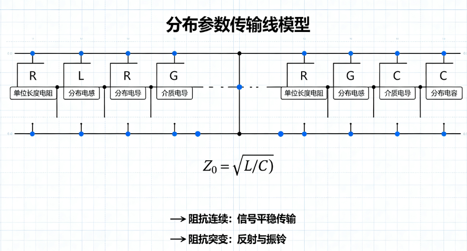
In high-speed circuits, PCB traces cannot be modeled as ideal wires; instead, they must be treated as distributed-parameter transmission line systems. Each infinitesimal segment of the trace inherently possesses distributed capacitance, inductance, conductor resistance, and dielectric conductance. These parameters are jointly determined by the trace geometry and PCB dielectric properties, and directly govern impedance performance.
1.1 Equivalent Physical Model of Transmission Lines
A transmission line can be decomposed into countless differential series segments. The per-unit-length equivalent circuit includes four core distributed parameters:
R: Conductor resistance per unit length (Ω/m)
L: Distributed inductance per unit length (H/m)
G: Dielectric leakage conductance per unit length (S/m)
C: Distributed capacitance per unit length (F/m)
When signal frequency ≥ 100 kHz or rise time is extremely short (rise time < 2× propagation delay), conductor resistance and dielectric leakage conductance can be neglected. The transmission line simplifies to a lossless model, with its characteristic impedance given by:
Z₀ = √(L/C)
Core Definition: Characteristic impedance is the ratio of voltage to current for a high-frequency forward-traveling wave. It depends solely on trace geometry and dielectric material, is independent of trace length and signal amplitude, and is an intrinsic electrical property of the transmission line.
1.2 Impedance Continuity and Signal Reflection Mechanism
The quality of high-speed signal transmission depends entirely on impedance continuity:
Impedance Continuity: Uniform and stable L and C parameters along the trace result in constant impedance, enabling smooth, distortion-free signal transmission.
Impedance Discontinuity: Changes in trace width, reference plane slots, via transitions between layers, or non-uniform dielectric thickness all cause abrupt Z₀ changes, leading to signal reflections, energy refraction, and impedance mismatch losses.
2. Core Classifications of PCB Transmission Lines
Based on transmission mode and reference structure relative to PCB layers, high-speed PCB transmission lines fall into multiple types, each with distinct electrical characteristics, impedance control logic, and application scenarios.
2.1 Classification by Signal Transmission Mode
2.1.1 Single-Ended Transmission Lines
Composed of a single signal trace with a ground reference plane forming the return path, this is the most basic transmission structure.
Limitations: Signal transitions easily induce ground bounce noise, interfering with adjacent traces, and exhibit weaker EMI immunity. Suitable for mid-to-low-speed control or auxiliary signals.
Impedance Behavior:
Proportional to the dielectric thickness between the trace and reference plane;
Inversely proportional to trace width and finished copper thickness;
Inversely proportional to the square root of the dielectric constant (εr).
2.1.2 Differential Transmission Lines
Consist of two equal-length, equal-width, parallel traces carrying symmetrical signals of equal amplitude but 180° out of phase. This is the dominant solution for modern high-speed signaling.
Key Advantages:
Common-Mode Noise Immunity: External noise couples equally onto both traces as common-mode signals, which are fully rejected by the differential receiver;
Low EMI Radiation: Opposing magnetic fields from the two traces cancel each other, resulting in minimal electromagnetic radiation—ideal for EMC compliance.
Engineering Note: Differential impedance is not simply the sum of two single-ended impedances; electromagnetic coupling between the traces must be considered. Smaller spacing increases coupling strength and lowers differential impedance.
2.2 Classification by PCB Layer Position and Physical Structure
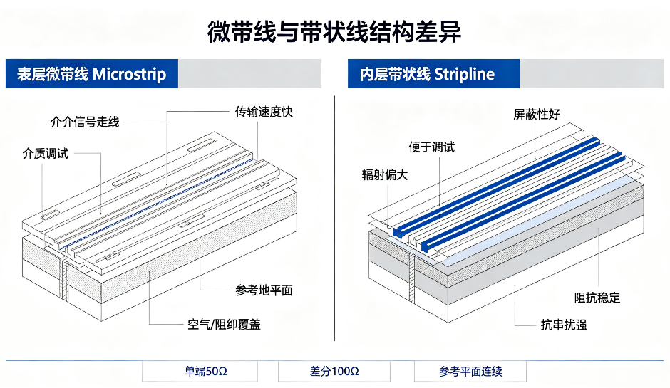
2.2.1 Outer-Layer Microstrip
Traces are placed on the PCB outer layer, with dielectric and reference plane on one side, while the top is exposed or covered with solder mask. This structure is simple and mature.
Advantages: Exposure to air results in a lower effective dielectric constant, reducing propagation delay and increasing speed; easy access for debugging and maintenance.
Disadvantages: Lack of upper shielding makes it susceptible to interference and results in higher radiation. Typically used for short-distance high-speed interconnects on outer layers.
2.2.2 Inner-Layer Stripline
Traces are embedded within inner PCB layers, surrounded by dielectric and flanked by reference planes on both sides.
Advantages: Dual ground planes provide natural shielding, excellent impedance continuity, strong crosstalk immunity, and superior stability.
Disadvantages: Encapsulation in dielectric results in a slightly higher effective dielectric constant, marginally reducing signal speed, and higher fabrication cost. Preferred for high-precision, high-frequency signals in inner layers.
3. Mainstream Transmission Line Structures and Engineering Implementation Forms
PCB etching processes produce trapezoidal cross-sections (narrower at the top). The industry universally uses the top trace width (W) as the baseline for impedance design, leading to five mainstream engineering structures.
3.1 Core Configurations for Single-Ended Impedance
Outer-Layer Microstrip: A basic, versatile structure with simple process, low cost, and low delay—suitable for most outer-layer single-ended high-speed signals.
Embedded Microstrip: Traces embedded in dielectric reduce air interference, improving impedance stability. Impedance is ~20% lower than standard microstrip, with reduced radiation—ideal for applications with basic EMI requirements.
Solder-Mask-Covered Microstrip: Outer-layer traces covered with solder mask (dielectric constant higher than air) reduce impedance by 2–3 Ω—a critical process parameter that must be calibrated in mass production.
Symmetric Stripline: Trace centered precisely between dual reference planes offers optimal electromagnetic symmetry and impedance consistency—ideal for ultra-high-frequency, low-jitter precision designs.
Offset Stripline: Unequal dielectric thickness above and below provides strong engineering tolerance and excellent manufacturability—the mainstream inner-layer structure for industrial multilayer boards.
3.2 Core Configurations for Differential Impedance
High-speed differential interfaces use edge-coupled structures, primarily in three forms:
Outer-Layer Differential Microstrip: Precise control of trace width and spacing enables accurate impedance tuning. Mature process and high yield make it suitable for standard high-speed differential interfaces like USB 3.0, HDMI, and Gigabit Ethernet.
Solder-Mask/Embedded Differential Microstrip: Optimizes coupling uniformity between traces, reduces impedance variation, and improves EMI and crosstalk performance.
Inner-Layer Differential Stripline: Dual-ground shielding provides exceptional crosstalk suppression and impedance stability—the preferred choice for premium applications like PCIe 4.0/5.0, 100G Ethernet, and DDR5 high-frequency clocks.
Reflected signals superimposed on the original signal cause overshoot, undershoot, ringing, and timing jitter—severely degrading performance or causing functional failure.
4. Standardized 50Ω / 100Ω Impedance Parameters for Mass Production (Ready-to-Use)
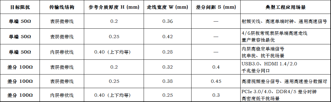
The table below summarizes mature, highly compatible standardized impedance parameters for 50Ω single-ended and 100Ω differential lines in industrial mass production. Calibrated for standard FR-4 materials, these values already account for etching and solder-mask-induced impedance reductions and can be directly applied in layout design.
Unified Calibration Baseline:
Material: Shengyi/Jiantao standard FR-4, dielectric constant εr = 4.4 at 1 GHz
Finished Copper Thickness: 1 oz (35 μm, including surface plating)
Standard Production Tolerance: ±5% (can be tightened or relaxed as needed)
Parameters already incorporate standard solder-mask impedance reduction—no secondary correction needed
Standardized Impedance Parameter Reference Table
Mass Production Calibration Rules
Solder Mask Correction: Solder mask coverage reduces impedance by 2–3 Ω—already accounted for in this table. For bare-copper (no solder mask) processes, reduce trace width by 0.01 mm to compensate.
Low-Loss Material Conversion: For low-dielectric materials like High-Tg, M4/M6 (εr ≈ 3.8–4.0), reduce trace width by 0.02–0.03 mm under the same thickness to maintain target impedance.
Tolerance Tier Management: Consumer products tolerate ±8%–±10%; industrial/high-precision equipment recommends ±5%; premium high-speed applications require ±3%.
Differential Hard Rules: 100Ω differential pairs must strictly maintain equal length, equal width, and parallel coupling. Prohibit single-trace routing, asymmetric layer transitions, or abrupt spacing changes.
5. Standardized Stack-Up Solutions for 4/6/8-Layer Boards (1.6 mm Standard Thickness)
Below are three industry-standard stack-up solutions based on 1.6 mm board thickness. These require no secondary lamination verification from the factory, offer high cost-effectiveness and broad compatibility, and can be directly used in project design.
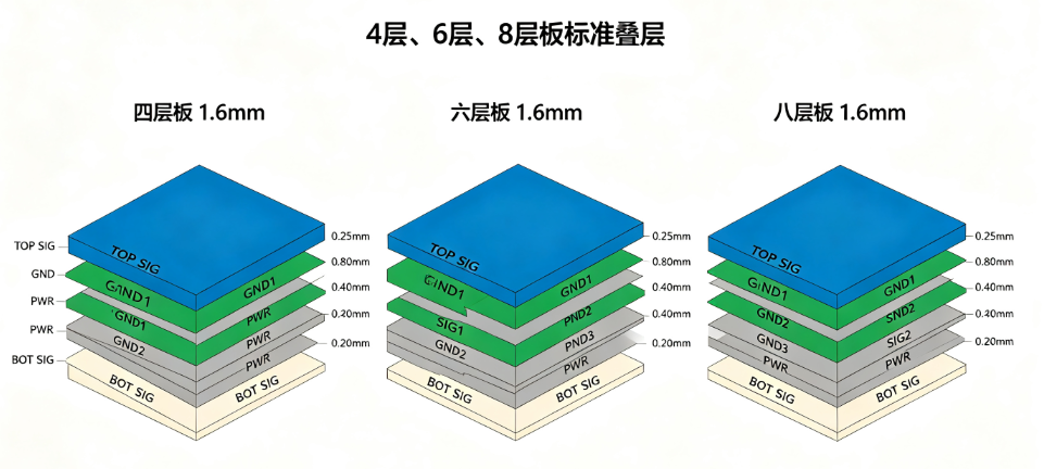
5.1 Four-Layer Standard Stack-Up (Cost-Effective Mass Production Standard)
Stack Structure: TOP(SIG) – GND – PWR – BOT(SIG)
Dielectric Layer Parameters:
TOP → GND: 0.25 mm (supports standard 50Ω/100Ω outer-layer impedance)
GND → PWR: 0.80 mm core prepreg (ensures power plane integrity)
PWR → BOT: 0.25 mm (supports bottom-layer microstrip impedance)
Design Rules: Route high-speed impedance-controlled signals on outer layers; keep inner planes intact. Never route impedance traces across plane splits to avoid return path disruption and impedance loss of control.
5.2 Six-Layer Standard Stack-Up (Industrial-Grade Shielding Optimization)
Stack Structure: TOP(SIG) – GND1 – SIG1 – PWR – GND2 – BOT(SIG)
Dielectric Layer Parameters:
TOP → GND1: 0.25 mm (standard outer-layer microstrip thickness)
GND1 → SIG1: 0.40 mm (optimal for inner-layer stripline impedance control)
SIG1 → PWR: 0.40 mm
PWR → GND2: 0.40 mm
GND2 → BOT: 0.25 mm
Design Rules: Route critical sensitive signals (e.g., PCIe, high-frequency clocks) on SIG1 inner layer to leverage dual-reference-plane shielding for superior crosstalk and EMI suppression—ideal for industrial mid-to-high-end equipment.
5.3 Eight-Layer Standard Stack-Up (Premium High-Speed, High-Stability Solution)
Stack Structure: TOP(SIG) – GND1 – SIG1 – GND2 – GND3 – SIG2 – PWR – BOT(SIG)
Dielectric Layer Parameters:
TOP/BOT outer-layer dielectric: 0.20 mm (enables fine narrow-trace impedance control)
SIG1/SIG2 inner-layer dielectric: 0.40 mm (symmetric stripline with excellent impedance consistency)
Design Rules: Multiple ground planes create a low-impedance return network; inner signal layers are fully isolated to eliminate inter-layer crosstalk—designed specifically for servers, high-speed data acquisition cards, and premium communication equipment requiring high stability and speed.
6. Golden Rules for Impedance Design and Mass Production Pitfall Avoidance
Combining theory and mass production practice, this section summarizes golden rules and key pitfalls across the entire impedance design workflow—from layout and process coordination to production verification—to effectively prevent hidden failure modes.
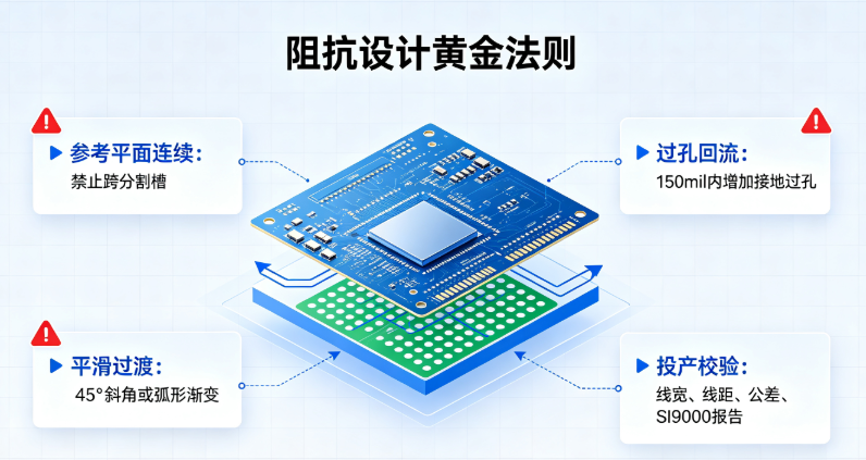
6.1 Reference Plane Continuity Rule (Highest Priority)
Impedance-controlled traces must be paired with complete, unslotted, uncut GND/PWR reference planes. Never route across splits or voids. Crossing splits elongates the return path, increases loop area, and directly causes impedance discontinuities, aggravated crosstalk, and EMI violations—the foremost taboo in high-speed design.
6.2 Via Transition Precision Control
Minimize layer transitions for high-speed traces. A single signal via introduces 0.5–1.0 pF parasitic capacitance and 1–2 nH parasitic inductance, disrupting impedance continuity and causing signal distortion and jitter. If layer transition is unavoidable, place grounding vias within 150 mils of the signal via to establish a continuous, symmetric return path and mitigate parasitic effects.
6.3 Smooth Trace Transition Design
When connecting impedance traces to IC pads, avoid right-angle transitions. Use 45° chamfers or curved tapers for smooth transitions to minimize impedance discontinuities from abrupt width changes, reducing signal reflections and ringing.
6.4 Pre-Production Verification Protocol
Before production, clearly specify impedance control requirements in the PCB fabrication specification to avoid impedance failures from process variations. Key points include:
Precisely annotate target impedance values, trace widths, and spacing for each layer;
Define impedance tolerance tiers for consumer, industrial, and premium applications;
Require the manufacturer to provide an SI9000 impedance simulation review report for verification before lamination.
This process effectively mitigates risks from stack-up mismatches, process deviations, and calculation errors, significantly improving first-pass yield and batch stability.
7. High-Frequency FAQ on PCB Impedance Control (Practical Q&A)
This section concisely addresses the top ten frequently asked questions in PCB impedance design, stack-up routing, and production release—eliminating fluff and delivering only actionable, field-tested conclusions to rapidly resolve real-world challenges and troubleshooting issues.
Q1: Why does measured PCB impedance deviate (high/low/out-of-spec) even when simulation parameters are correct?
A: Primarily due to process and material variations—not design errors. Dielectric constant shifts, lamination thickness tolerances, copper foil roughness, and solder mask coverage (typically reducing impedance by 2–5 Ω) all cause measurement deviations. Allow ±5% tolerance for standard applications and ±3% for premium scenarios; align material and copper thickness specs with your PCB vendor before production to avoid issues.
Q2: When is impedance control mandatory? Do low-speed signals need it?
A: Not all traces require impedance control. High-speed signals with frequency ≥100 MHz or edge rates ≤1 ns (e.g., DDR, PCIe, HDMI, USB 3.0, high-frequency clocks, Gigabit Ethernet) must be impedance-controlled; standard GPIO, low-speed control lines, and power traces do not require matching.
Q3: Why do 100Ω differential pairs still exhibit packet loss or instability despite correct width/spacing?
A: Differential impedance relies on symmetric coupling + complete return path—matching width/spacing alone is insufficient. Unequal lengths, spacing offsets, asymmetric routing, local width variations, or reference plane splits introduce excessive common-mode noise, causing communication errors or screen artifacts. Fix: Maintain strict parallel, equal-distance, symmetric routing throughout; never route one trace independently; ensure reference plane integrity.
Q4: Can impedance traces change layers or use vias? What issues arise from layer transitions?
A: High-speed impedance traces should preferably stay on a single layer—avoid arbitrary layer changes. Transitions disrupt return paths and alter dielectric environments, causing impedance discontinuities, reflections, and timing skew. If layer change is unavoidable, add nearby ground vias to shorten the transition zone and maintain consistent trace parameters.
Q5: Which offers better impedance stability for high-speed signals—outer-layer microstrip or inner-layer stripline?
A: Inner-layer stripline is far more stable than outer-layer microstrip. Its dual-ground shielding and enclosed dielectric environment minimize crosstalk and ensure excellent impedance consistency—ideal for precision high-speed signals like PCIe and DDR4/5. Microstrip, being exposed, is more susceptible to interference and radiates more—suitable only for standard high-speed interfaces.
Q6: What are standard PCB impedance tolerances? How to select for different applications?
A: Industry tolerance tiers are well-defined and ready to apply: ±10% for low-speed general-purpose boards; ±5% for standard high-speed signals (USB, HDMI, DDR—parameters in this document are calibrated for this); ±3% for servers, RF, and high-precision circuits.
Q7: Why do impedance discontinuities occur even with a complete reference plane?
A: Even with a solid reference plane, pad width transitions, local trace narrowing/widening, via stubs, etching non-uniformity, or localized dielectric thickness variations can cause local impedance jumps. Ensure smooth transitions using 45°/curved traces, minimize pad extensions, and avoid abrupt structural changes.
Q8: Can impedance parameters be interchanged between 4-layer and 6-layer stack-ups? Are parameters transferable across different board thicknesses?
A: No—never interchange or mix parameters. Impedance is determined by dielectric thickness and layer structure. 0.20 mm/0.25 mm outer-layer dielectrics have dedicated microstrip parameters; 0.40 mm inner-layer dielectrics have dedicated stripline parameters. Mixing across stack-ups or thicknesses will directly cause impedance violations.
Q9: Does solder mask opening improve impedance accuracy? When is it needed?
A: Solder mask slightly lowers outer-layer impedance; opening windows eliminates this effect, improving simulation-to-measurement consistency. Recommended for premium RF 50Ω and high-speed 100Ω differential signals; unnecessary for standard industrial/consumer electronics—parameters in this document already account for standard solder mask tolerances.
Q10: Can single-ended 50Ω and differential 100Ω traces share the same layer? What precautions are needed?
A: Yes, but strict isolation is required: never run the two types parallel over long distances; maintain spacing ≥3× trace width; strictly separate microstrip/stripline parameters and avoid mixing widths. Optimal approach: route differential high-speed signals on inner layers and single-ended signals on outer layers—segregate by layer and zone to prevent crosstalk.
trending news
Contact Us