



Sorry, no sales person is available right now to take your call. Pls leave a message and we will reply to you via email as soon as possible.
Home/ PCB News/ Core Principles of PCB Stack-up Design and Selection Guide for 6/8-Layer Boards
Core Principles of PCB Stack-up Design and Selection Guide for 6/8-Layer Boards
2026-07-20
There is no "universal formula" for PCB stack-up design; the optimal solution must be a comprehensive trade-off based on three key factors: signal type, component layout density, and project cost. Regardless of the architecture adopted, three core principles must always be adhered to, ensuring signal integrity (SI), electromagnetic compatibility (EMC), and mechanical stability of the board:
Symmetrical structure—prevents board warpage and ensures manufacturing yield;
Tight coupling between signal layers and reference planes—shortens return paths and maintains impedance continuity;
Physical isolation between power/ground planes and signal layers—reduces power noise coupling and enhances noise immunity.
I. 6-Layer Board Design: Mainstream Solutions and "Pseudo-8-Layer" Technology
The 6-layer board offers a balance of routing flexibility and cost efficiency, making it a common choice for mid-to-low-end high-density PCBs. Below are three standardized stack-up schemes, along with a performance-enhancement path via "pseudo-8-layer" technology.
1. Mainstream Stack-Up Schemes (Visual Structure Illustration)
Color legend: Blue – Signal layers | Green – GND plane | Orange – VCC power plane (stacking order shown from top to bottom)
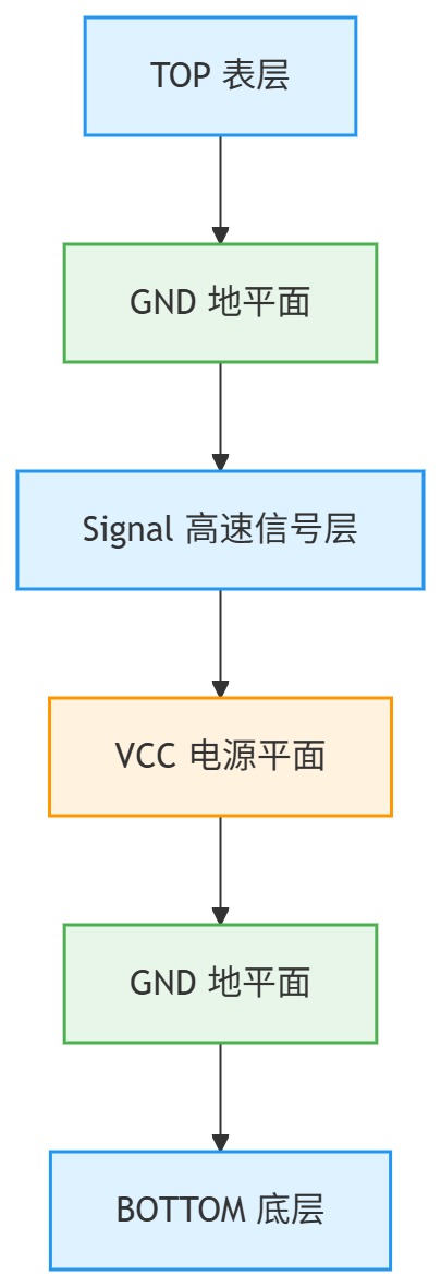
Features: High-speed internal signals are fully "sandwiched" between solid ground planes above and below, forming a shielded cavity. This provides the shortest return path, excellent impedance continuity, and superior suppression of radiation and external interference—making it the preferred architecture for high-speed designs (e.g., DDR, Gigabit Ethernet).
Color legend: Blue – Signal layers | Green – GND plane | Orange – VCC power plane (stacking order shown from top to bottom)
Features: High-speed internal signals are fully "sandwiched" between solid ground planes above and below, forming a shielded cavity. This provides the shortest return path, excellent impedance continuity, and superior suppression of radiation and external interference—making it the preferred architecture for high-speed designs (e.g., DDR, Gigabit Ethernet).
6-Layer Board Scheme B (Cost-Optimized · High-Density Routing)
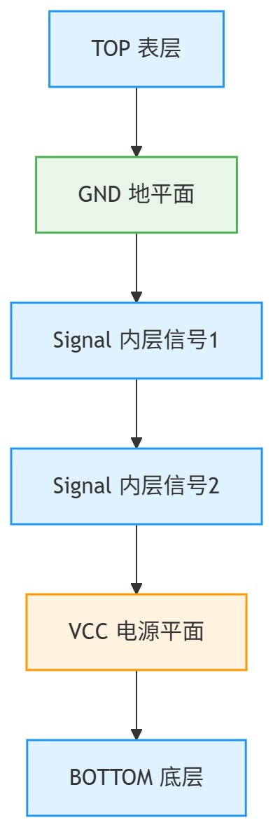
Features: Offers four usable signal layers—the most routing resources—and lower cost, ideal for consumer electronics with extremely high component density and tight routing constraints. Drawback: Higher risk of crosstalk between adjacent internal signal layers, which must be mitigated by increasing trace spacing, using orthogonal routing directions, and minimizing parallel run lengths.
6-Layer Board Scheme C (Entry-Level HDI Simplified Stack-Up)
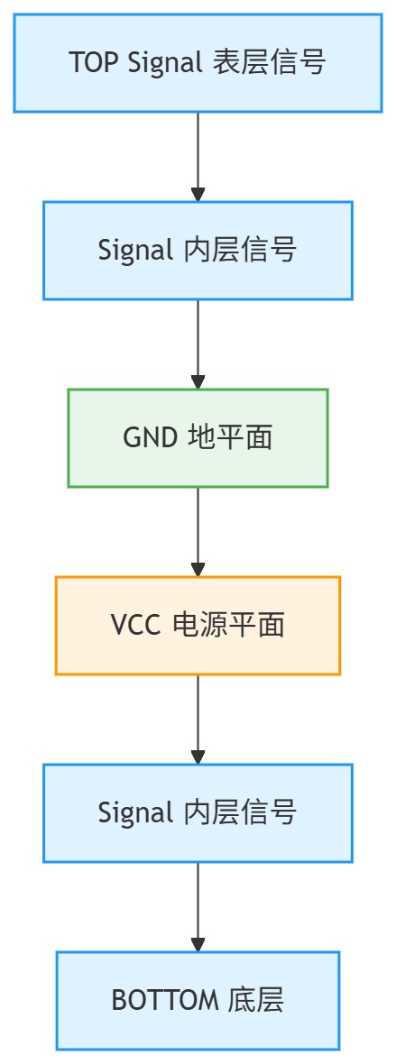
Features: The top layer lacks an adjacent reference plane, leading to significant cross-interference between inner and outer signals and making SI control challenging. Suitable only for low-speed, low-performance basic HDI products; not recommended for high-speed or precision circuits.
2. "Pseudo-8-Layer" Technology—A Shortcut to Enhanced Performance
By increasing the core substrate thickness in a 6-layer board and combining it with optimized trace width and precise impedance tuning, electrical performance approaching that of an 8-layer board can be achieved—without increasing layer count or significantly raising costs. This approach is especially suitable for high-density BGA layouts, balancing dense routing with effective shielding.
3. Recommended Material Configuration (Standard 1.6mm Board Thickness)
Use a combination of two 0.3mm core laminates + three sheets of 1080 prepreg , which provides high structural symmetry, stable impedance characteristics, and effectively prevents warpage—ideal for most standard 6-layer designs.
II. 8-Layer Board Design: For Complex, High-Performance Systems
The 8-layer board provides abundant layer resources, enabling independent isolation of multiple power domains and layered signal management—effortlessly handling complex scenarios such as high-speed buses, mixed-signal (analog/digital) integration, and multi-module systems.
1. Mainstream Stack-Up Schemes (Visual Structure Illustration)
Scheme A (Balanced General-Purpose · All-Scenario Compatible)
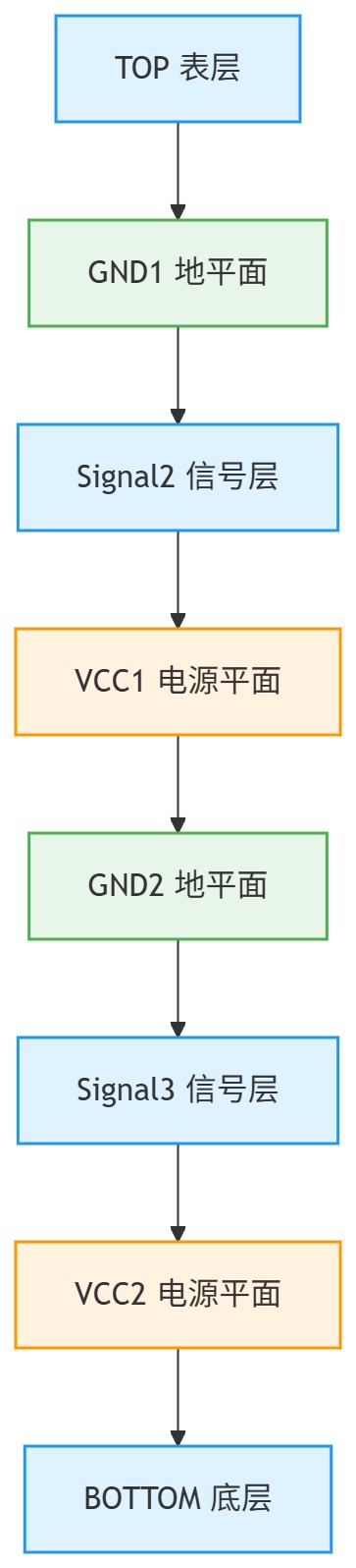
Features: Four signal layers paired with two independent power/ground plane pairs offer a balanced structure, enabling separate routing zones for digital and low-speed analog signals. Widely used in industrial control motherboards, mid-range servers, and smart device main controllers—ideal for typical mixed-signal high-performance applications.
8-Layer Board Scheme B (High-Speed Dense · Dedicated to High-Speed Buses)
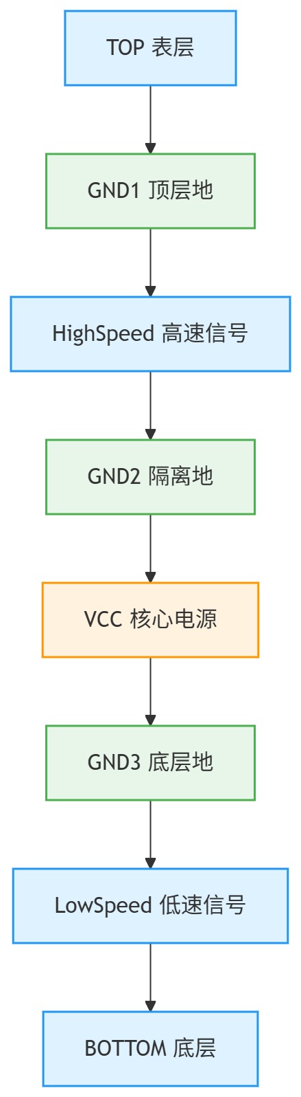
Features: High-speed signals are fully enclosed in a "GND–High-Speed–GND" sandwich structure, resulting in extremely short return paths and optimal crosstalk and radiation suppression—effectively resolving SI issues in high-speed buses. Low-speed signals are routed on dedicated layers, preventing interference between high- and low-speed domains. This is the ideal solution for PCIe, DDR, and similar interfaces.
Scheme C (Advanced Customization · Complex System Tailoring)
No fixed standard architecture; layer assignments can be flexibly customized based on requirements such as RF/analog mixed-signal integration, multi-power-domain isolation, or any-layer HDI. Suitable for high-end industrial control, RF equipment, and precision instruments demanding high integration and stringent isolation.
2. Recommended Material Configuration (0.8mm Thin Board Thickness)
Use three 0.2mm thin core laminates + four sheets of 106 prepreg for a lightweight yet structurally stable stack-up, compatible with high-density fine routing and microvia HDI processes—meeting the demands of miniaturized, highly integrated designs.
III. 6-Layer vs. 8-Layer: Selection Decision Comparison
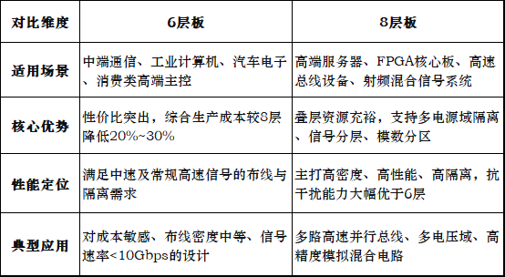
Recommendation: If the project is cost-sensitive and involves moderate signal speeds, a 6-layer board (especially Scheme A or the pseudo-8-layer approach) is optimal. However, for designs involving complex high-speed interfaces, multi-power-domain management, or stringent EMC requirements, an 8-layer board should be selected directly to ensure sufficient design margin and reliability.
trending news
Contact Us