



Sorry, no sales person is available right now to take your call. Pls leave a message and we will reply to you via email as soon as possible.
Home/ PCB News/ In-Depth Analysis of Core Technical Challenges in Ceramic Metallization
In-Depth Analysis of Core Technical Challenges in Ceramic Metallization
2026-07-16
Ceramic substrates, with their excellent properties such as high thermal conductivity, high electrical insulation, high-temperature resistance, and low coefficient of thermal expansion (CTE), have become fundamental carrier materials in high-end fields including power semiconductors, optoelectronic packaging, microwave/RF applications, and new energy storage. However, ceramics are inorganic materials bonded by ionic/covalent bonds, whereas metals are conductors held together by metallic bonds—creating an inherent barrier between them in terms of physical properties and interfacial characteristics. Ceramic metallization, the key process enabling reliable ceramic-to-metal joining, has long faced multidimensional technical bottlenecks related to materials, interfaces, processing, and reliability. These challenges directly impact the yield and long-term operational stability of ceramic substrate products such as DBC, AMB, DPC, Mo-Mn thick-film, and HTCC. This article systematically analyzes the pain points across the entire ceramic metallization process from four perspectives: fundamental material contradictions, interfacial bonding mechanisms, process control, and end-application reliability. It identifies the root causes of these underlying conflicts and, through real-world industry case studies, concretely demonstrates the technological value and engineering challenges.
I. Fundamental Material Conflict: Inherent Physical Property Mismatch Between Ceramics and Metals
The root cause of all challenges in ceramic metallization lies in the intrinsic differences in physical and chemical properties between these two material classes—a fundamental and unavoidable constraint.
1. Severe Mismatch in Coefficient of Thermal Expansion (CTE)
Ceramics such as alumina (Al₂O₃), aluminum nitride (AlN), and silicon nitride (Si₃N₄) exhibit extremely low CTE values, while conductive metals like copper, nickel, and silver have CTEs several times higher. During cooling after high-temperature sintering or brazing, the mismatch in contraction rates generates significant residual thermal stress at the interface. This issue is particularly pronounced in thick-copper DBC and AMB substrates and large-format ceramic boards, directly causing warpage, ceramic cracking, metal layer delamination, and interfacial separation after thermal cycling.
2. Chemical Inertness of Ceramic Surfaces Prevents Wetting by Molten Metals
Ceramics, bonded by ionic and covalent bonds, possess very low surface chemical activity, making it difficult for molten solders or liquid metals to wet and spread—thus preventing physical adhesion. The industry commonly introduces reactive transition metals such as Ti or Cr, which react with ceramics at high temperatures to form intermediate phases (e.g., titanates, aluminates) that act as bonding bridges. Without such an active transition layer, the adhesion between metal and ceramic approaches zero, leading to easy delamination under minimal mechanical stress.
3. Porosity and Density Variations in Ceramics Introduce Latent Defects
Conventionally sintered ceramics often contain micro-pores and exhibit non-uniform surface roughness, introducing multiple quality risks: during high-temperature metallization, molten metal infiltrates pores, forming internal micro-cracks that accelerate propagation under stress; trapped gases within pores slowly outgas during subsequent packaging, compromising hermeticity; and during electroplating, pores cause voids in the plated layer, increasing adhesion variability and reducing batch-to-batch consistency.
II. Interfacial Bonding: The Core Microscale Control Challenge Across the Entire Process
The bond strength between ceramic and metal critically depends on the microstructure of the interfacial reaction layer, which has an extremely narrow tolerance window—widely recognized as the core technical barrier in the industry.
1. Difficulty in Precisely Controlling Interfacial Chemical Reactions
The essence of metallization lies in forming stable solid solutions or ceramic intermediate phases (e.g., titanates, aluminates) at the interface. The reaction outcome is highly sensitive to sintering temperature, atmosphere, and dwell time. Minor fluctuations can lead to two extreme failure modes: insufficient reaction yields too little intermediate phase, resulting in poor adhesion and easy metal peeling; excessive reaction generates brittle compounds, reducing interfacial toughness and causing brittle fracture during thermal cycling, thereby degrading thermal shock resistance.
2. Extremely Narrow Thickness Window for Transition Layers
Ti, Mo, Mn, and similar elements are commonly used as base transition layers. Their thickness directly determines bonding performance: if too thick, overall brittleness increases and impact resistance decreases; if too thin, a continuous and complete reaction bridge cannot form, leading to adhesion failure. Transition layer thickness is typically controlled at the nanometer to micrometer scale, making uniformity across the entire substrate and consistency across production batches extremely difficult to achieve. Minor thickness variations can cause significant performance divergence within the same batch.
3. Interlayer Mismatch in Multilayer Metal Stacks
Mature processes employ multilayer metal structures: an active base layer (Ti/Cr/Mo) + a diffusion barrier layer (Ni) + a solderable top layer (Cu/Au/Ag). At elevated temperatures, interdiffusion and intermetallic compound formation occur between layers, generating brittle phases that ultimately cause metal layer blistering, delamination, or solder joint detachment—leading to batch-level failures.
III. Process Technology: Extremely Low Tolerance Across All Process Steps
From high-temperature sintering and patterning to electroplating and post-treatment, every process step has an extremely narrow operating window. Minor fluctuations in equipment, environment, or raw materials can trigger mass defects.
1. Extremely Narrow Control Window for Sintering Atmosphere and Temperature
Different technology routes impose strict requirements on temperature profiles and atmospheres with minimal allowable variation: Mo-Mn thick-film and HTCC processes require weakly reducing H₂/N₂ atmospheres, where a temperature fluctuation beyond ±10℃ alters adhesion and hermeticity; DBC direct bonding relies on a narrow Cu-O eutectic reaction window, where trace oxygen variations cause poor bonding or copper over-oxidation; AMB active metal brazing demands high vacuum, and imbalances in thermal profiles or ramp rates directly induce ceramic cracking.
2. Challenges in Controlling Pattern Accuracy and Edge Uniformity
Thick-film printing, DBC, and AMB processes often produce line burrs, bleeding, breaks, and linewidth deviations. Although DPC thin-film processes offer higher precision via photolithography and sputtering, they demand extreme equipment accuracy and cleanroom conditions, resulting in high production costs. For high-power and high-frequency devices, stringent specifications on linewidth, line spacing, and metal edge verticality mean that even minor patterning defects significantly reduce yield.
3. Plating Stress and Pinhole Defects in Electroplated Layers
Post-metallization nickel/gold plating is required for solderability, but electroplating often introduces two typical defects: excessive internal stress in the plated layer pulls on the underlying metal, causing substrate warpage or delamination; surface contamination or micro-pores on the ceramic lead to pinholes or localized missed plating, resulting in poor solder joints and reduced corrosion resistance.
4. High-Temperature Deformation of Large, Thin Ceramic Substrates
Current mainstream power device ceramic sheets are only 0.25–0.6 mm thick, and demand for larger substrates continues to grow. After high-temperature metallization, they are highly prone to warpage, bowing, or wavy distortion. Excessive deformation renders them incompatible with downstream die-attach and assembly processes, leading to direct scrap.
IV. Reliability and End-Use Applications: Rigorous Demands of Service Environments
Ceramic metallized substrates must operate reliably under harsh conditions such as thermal cycling, vacuum hermeticity, and high-frequency wire bonding. Achieving consistent reliability in mass-produced products remains the greatest challenge for real-world deployment.
1. Interfacial Fatigue Failure Under Thermal Cycling and Thermal Shock
Power devices typically operate across a temperature range of -40℃ to 125℃. Repeated cycling induces cyclic stress from CTE mismatch, gradually causing metal layer fatigue, interfacial microcracks, and eventual debonding—making this the most common failure mode in power device manufacturing.
2. High Hermeticity Requirements Pose Major Inspection and Control Challenges
Microwave waveguides, laser devices, and vacuum hermetic housings demand extremely low leak rates. Microscopic cracks or gaps are invisible to the naked eye and require specialized leak detection equipment. Any interfacial micro-defect can cause leak rate failures, making defect control across the entire process highly challenging.
3. Inconsistent Wire Bonding and Solderability
Variations in surface roughness, oxidation level, and plating thickness of the metallized layer directly affect downstream packaging: insufficient pull strength in gold/aluminum wire bonding leads to bond lifting; poor solder wetting in SMT causes voids, significantly reducing packaging yield.
4. Poor Batch-to-Batch Consistency Hinders Yield Improvement
Final metallization performance is influenced by multiple coupled factors—including ceramic green body batches, metal paste composition, furnace thermal profiles, and cleanroom conditions. Minor fluctuations in any parameter can cause adhesion scatter, cracking, or leakage, making stable high yield in mass production a persistent engineering challenge.
V. Summary of Root Causes Behind Technical Challenges
Synthesizing all process pain points, the technical bottlenecks in ceramic metallization can be distilled into three core root causes:
Fundamental Material Incompatibility—The inherent mismatch in CTE and chemical bonding nature between ceramics and metals makes stress and wetting issues impossible to fully eliminate at the material level.
Microscale Interfacial Instability—Interfacial reactions, transition layer thickness, and multilayer metal diffusion all occur at microscopic scales, making precise parameter control extremely difficult; minor variations significantly alter bond strength.
Narrow Process Windows Coupled with Stringent Reliability Standards—Sintering temperature, atmosphere, and ramp rates have minimal tolerance, while end-use applications demand simultaneous validation for thermal cycling, hermeticity, and bonding/soldering performance—multiplying process control complexity.
VI. Key Industry Application Case Studies
As a foundational enabler in advanced electronics manufacturing, ceramic metallization empowers diverse sectors including telecommunications, power semiconductors, optoelectronics/lasers, medical devices, and automotive/aerospace systems. Each application leverages tailored process routes to address core needs such as electrical insulation, heat dissipation, hermetic sealing, and high-frequency signal transmission—while vividly illustrating the aforementioned interfacial control and process stability challenges. All case parameters below adhere to industry-standard specifications and mass-production validation protocols to ensure data rigor and traceability.
1. 5G/6G High-Frequency Substrate Applications (DPC Thin-Film Metallization)
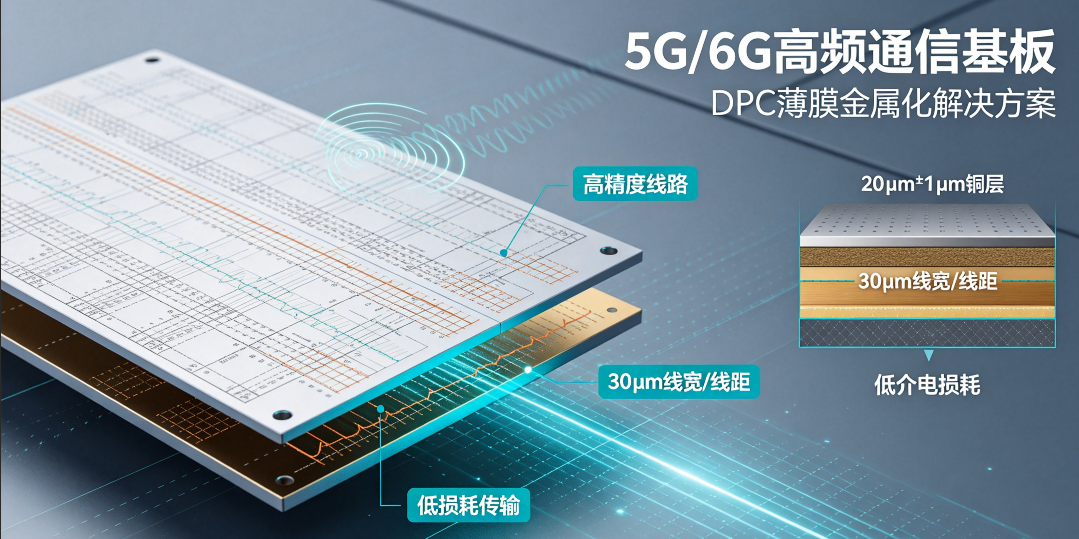
5G macro base stations and high-speed optical communication modules demand ultra-low RF loss, high-precision circuitry, and superior thermal management—areas where traditional organic PCBs fall short due to high dielectric loss and poor thermal stability. Baineng Yunban has developed and commercialized an AlN ceramic substrate solution using proprietary high-precision DPC thin-film metallization. Through magnetron sputtering, a high-purity copper conductive layer of 20 μm ±1 μm is precisely deposited on AlN substrates, enabling stable fabrication of 30 μm ultra-fine line/space features. The low dielectric loss effectively minimizes high-frequency signal attenuation and controls temperature rise. With 36 standardized quality control steps throughout the process and Ni/Pd/Au plating for post-treatment, defects such as pinholes, oxidation, and thickness non-uniformity are eliminated. The substrate maintains electrical performance variation below 1% under long-term high-frequency operation, fully meeting the reliability requirements of 5G baseband modules and high-speed optical transmission equipment.
2. New Energy Automotive Power Module Applications (AMB Active Metal Brazing)
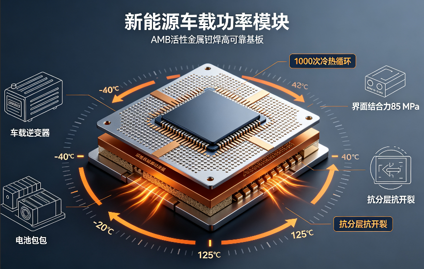
Power devices in electric vehicle ECUs, OBCs, and photovoltaic inverters operate under extreme conditions: -40℃ to 125℃ thermal cycling, high vibration, and heavy loads—demanding exceptional interfacial resistance to thermal shock and delamination. Baineng Yunban has developed a proprietary low-temperature AMB process for automotive applications, producing Si₃N₄-based AMB metallized substrates. By precisely controlling vacuum sintering temperature profiles, maintaining constant vacuum levels, and standardizing ramp rates, excessive brittle phase formation is suppressed, optimizing interfacial stress matching and bond toughness. The copper-ceramic interfacial bond strength reaches 85 MPa—significantly exceeding the industry average of 62 MPa. Certified by authoritative automotive reliability tests, mass-produced substrates reliably pass over 1,000 cycles (up to 2,000+ in upgraded versions) of -40℃ to 125℃ thermal cycling without delamination, cracking, or metal peeling, and are now in volume supply to leading domestic automakers and energy storage companies.
3. High-Power Laser and Optoelectronic Packaging (Mo-Mn Thick-Film + Au-Sn Eutectic Metallization)
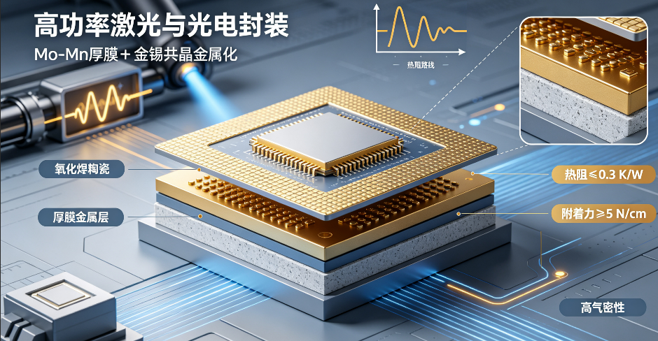
Industrial high-power lasers, high-speed optical modules, and automotive LiDAR BAR chip arrays demand ceramic carriers with hermeticity, low thermal resistance, and long-term high-temperature stability. Baineng Yunban leveraged mature Mo-Mn thick-film technology to deliver a 96% Al₂O₃ metallization solution for TRUMPF’s 3 kW industrial semiconductor laser project. By precisely controlling hydrogen reduction atmosphere, temperature, and dwell time during sintering, a uniform and dense transition interface was formed, ensuring target adhesion and hermeticity. Combined with Au-Sn eutectic soldering, the total thermal resistance is ≤0.3 K/W, effectively handling localized high-temperature loads from laser operation and resolving interfacial delamination and power degradation issues. Through continuous optimization of paste formulation and sintering parameters, metallization layer adhesion is stably maintained at ≥5 N/cm with batch variation within ±0.2 N/cm, achieving industry-leading yield and enabling volume production for 10 Gbps optical modules and industrial laser systems.
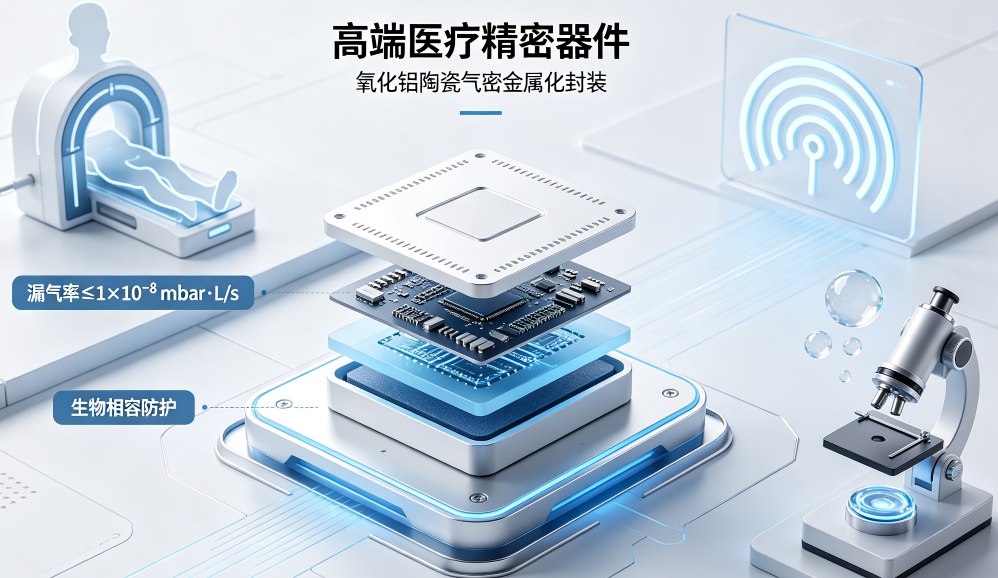
4. High-End Medical Precision Device Applications (Hermetic Alumina Metallization)
Implantable medical devices and advanced imaging diagnostic equipment require medical-grade standards for insulation, corrosion resistance, biocompatibility, and hermeticity. Baineng Yunban developed customized 96% Al₂O₃ Mo-Mn hermetic packaging substrates for implantable devices such as pacemakers and cochlear implants. Using high-precision high-temperature sintering, a dense, defect-free metallized sealing layer was fabricated, providing reliable electrical isolation between internal circuits and human tissue. Medical-grade hermeticity testing confirms leak rates consistently ≤1×10⁻⁸ mbar·L/s, ensuring long-term resistance to bodily fluid ingress and preventing internal oxidation or corrosion. The product passes biocompatibility and high-temperature sterilization tests, remaining stable under MRI/CT electromagnetic fields and repeated sterilization cycles—without deformation, leakage, or aging—making it a core enabler for domestic substitution in high-end medical electronics.
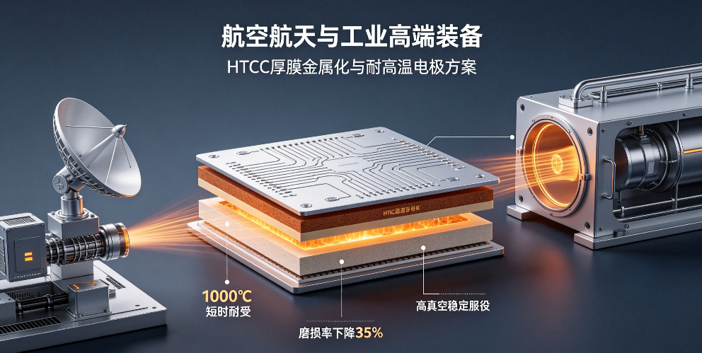
5. Aerospace and Industrial High-End Equipment Applications
Aerospace airborne radars, engine temperature sensors, and advanced plasma coating equipment impose extreme demands on ceramic metallized components for high-temperature resistance, anti-aging properties, and environmental stability. Baineng Yunban leverages a full portfolio of HTCC, LTCC, DBC, and AMB processes to precisely meet these rigorous requirements. Mass-produced HTCC thick-film metallized substrates withstand short-term exposure to 1000℃, maintaining signal integrity, interfacial integrity, and dimensional stability in vacuum, strong EMI, and thermal cycling environments. Addressing rapid electrode wear in industrial plasma coating systems, a proprietary Ag-Pd ceramic metallized electrode overcomes the high-temperature oxidation and wear limitations of conventional pure-metal electrodes, reducing high-temperature wear by 35% and extending continuous service life from 3 to over 5 months—significantly lowering maintenance costs and becoming the preferred solution for domestic high-end equipment upgrades.
Ceramic metallization serves as the critical bridge connecting insulating ceramic substrates with conductive metal circuits. Its technical challenges span the entire chain—from materials and interfaces to processing and reliability. Real-world applications in 5G/6G communications, new energy automotive power systems, high-power lasers/optoelectronics, medical devices, and aerospace clearly demonstrate that capabilities in interfacial precision control, process stability, and stress matching directly determine the performance ceiling, yield, and long-term service life of advanced electronic devices. With rapid advancements in third-generation semiconductors, new energy storage, and high-speed optical interconnects, demand continues to rise for large-format, ultra-thin, high-precision, and highly reliable ceramic substrates. Future R&D in ceramic packaging will focus on fundamentally balancing material property conflicts, achieving microscale interfacial precision, and widening robust mass-production process windows.
trending news
Contact Us