



Sorry, no sales person is available right now to take your call. Pls leave a message and we will reply to you via email as soon as possible.
Home/ PCB News/ High-Frequency RF (Rogers) PCB Design and Manufacturing Process Technical Specification
High-Frequency RF (Rogers) PCB Design and Manufacturing Process Technical Specification
2026-07-17
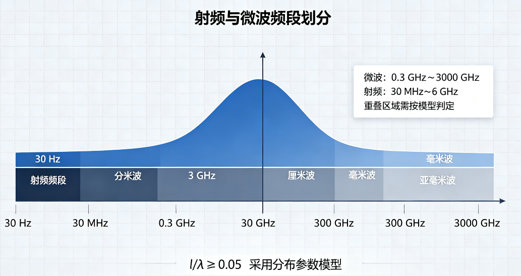
1. Definition and Frequency Band Division of Microwaves and Radio Frequency Electromagnetic Waves
Microwaves are electromagnetic waves defined based on the electromagnetic spectrum, with a wavelength range of 1 m to 0.1 mm, corresponding to a frequency range of 0.3 GHz to 3000 GHz. This band can be further divided into four sub-bands (including the upper limit but excluding the lower limit): decimeter waves (0.3 GHz–3 GHz), centimeter waves (3 GHz–30 GHz), millimeter waves (30 GHz–300 GHz), and sub-millimeter waves (300 GHz–3000 GHz). It should be noted that some industry literature excludes the sub-millimeter wave band from the definition of microwaves. Microwaves exhibit five typical physical characteristics: light-like behavior, sound-like behavior, penetrability, non-ionizing nature, and information-carrying capability.
Radio frequency (RF) refers to a category of electromagnetic waves defined for engineering applications, specifically those suitable for radio communication. There is no fully unified industry standard for its frequency band division; mainstream definitions typically specify either 30 MHz–3 GHz or 300 MHz–40 GHz, which overlaps with the microwave band. From the perspective of spectrum division, RF electromagnetic waves have a wavelength range of 1000 m to 1 m, corresponding to a frequency range of 30 Hz to 300 MHz. There is no strict rigid boundary between RF and microwaves, and this boundary continues to evolve dynamically with advancements in semiconductor processes and PCB design technologies. The high-frequency RF PCBs referenced in this specification refer specifically to specialized high-frequency printed circuit boards designed for RF-band signals and particularly those fabricated using Rogers high-frequency laminates.
2. Frequency Band Definition and Circuit Model Selection Criteria for High-Frequency RF PCBs
The transmission line circuit models for high-frequency RF PCBs are categorized into lumped-parameter models and distributed-parameter models. In engineering practice, the critical criterion
ll/λ≥0.05 is used as the basis for distinction, where ll is the geometric length of the transmission line and λλ is the operating wavelength of the signal.
This specification stipulates: any RF analog signal transmission line circuit employing a distributed-parameter model shall be collectively referred to as an RF link.
Considering practical engineering scenarios, the maximum geometric trace length on conventional RF PCBs typically does not exceed 50 cm, corresponding to a minimum design-controlled frequency of approximately 30 MHz. The industry commonly defines frequencies above 3 GHz as pure microwave bands, which may serve as a reference for the upper frequency limit in conventional RF PCB designs. Additionally, considering the manufacturing process limits for mass production (minimum component spacing of 0.5 mm), the theoretical maximum applicable frequency can reach up to 30 GHz. However, this ultra-high-frequency band offers limited practical reference value for conventional RF PCB engineering design and is therefore not included within the standard controlled frequency range of this specification.
Taking into account frequency band overlap characteristics, engineering practicality, and compatibility with mass production processes, this specification explicitly defines the applicable signal frequency range for high-frequency RF (Rogers) PCBs as 30 MHz to 6 GHz for analog RF signals. Circuit model selection must strictly follow the
l/λ≥0.05l/λ≥0.05 criterion, flexibly selecting either a lumped-parameter or distributed-parameter model based on actual trace length and operating wavelength.
3. Technical Requirements for High-Frequency PCB Substrate and Conductor Materials
Rogers high-frequency laminates have a relatively high dielectric constant, resulting in slower electromagnetic wave propagation speeds within the dielectric compared to free space. Consequently, at the same frequency, the operating wavelength inside the dielectric is shorter, significantly increasing the sensitivity of signal transmission to the physical and electrical parameters of both the substrate and conductors. Therefore, high-frequency PCBs impose far stricter material performance accuracy requirements than standard PCBs.
3.1 Dielectric Substrate (Rogers High-Frequency Laminate) Requirements
Rogers high-frequency dielectric substrates must meet the following core specifications:
Extremely low dielectric loss tangent, with stable dielectric constant across the rated operating frequency and temperature range, showing no significant drift;
High thermal conductivity and high surface flatness;
Strong adhesion to copper foil conductor layers, excellent bonding stability, capable of reliably carrying high-frequency signals over extended periods without signal attenuation, phase distortion, or transmission anomalies caused by parameter fluctuations.
3.2 Conductor Metal Material Requirements
PCB conductor copper foil materials must satisfy the following:
High conductivity and low temperature coefficient of resistance to minimize high-frequency transmission losses;
Excellent adhesion to the dielectric substrate, free from delamination, peeling, or flaking defects;
Good solderability compatible with standard reflow soldering, press welding, and ultrasonic bonding processes, ensuring long-term reliability of device solder joint electrical connections.
4. Core Guidelines for High-Frequency RF PCB Trace Design
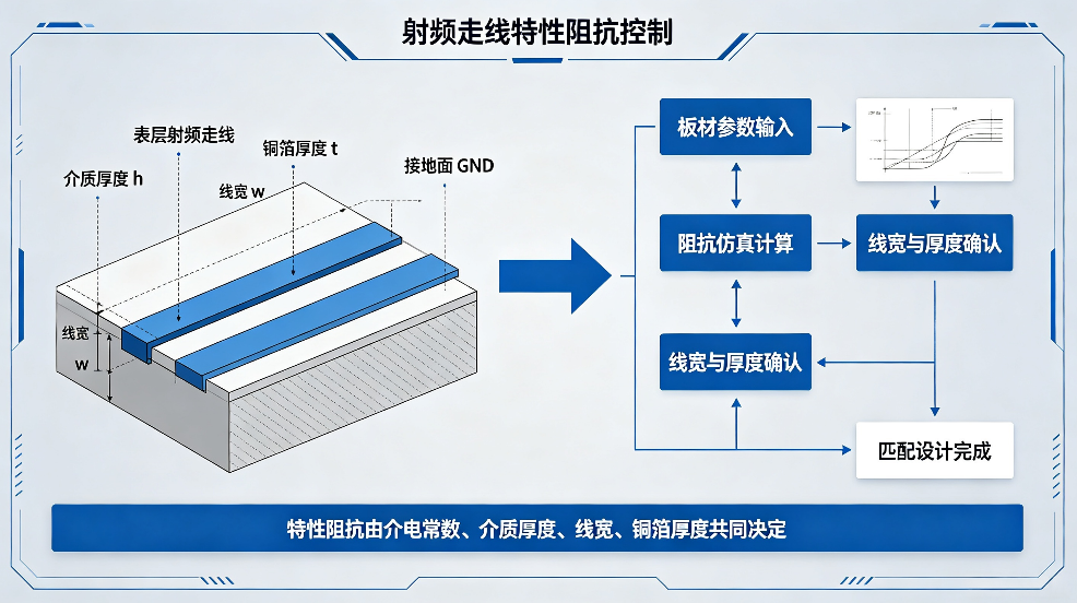
In addition to meeting general PCB requirements for determining trace width based on current-carrying capacity, the core control points for high-frequency RF PCB trace design lie in characteristic impedance control and precise impedance matching. High-frequency RF signals are highly sensitive to impedance deviations; impedance mismatches directly cause signal reflections, increased insertion loss, waveform distortion, and excessive VSWR. Therefore, precise control of trace characteristic impedance must be maintained throughout both design and manufacturing stages.
The characteristic impedance of traces is jointly determined by parameters including the laminate’s dielectric constant, dielectric thickness, trace width, and copper foil thickness. Designers must thoroughly understand the electrical and physical parameters of Rogers high-frequency laminates to achieve accurate impedance-matched designs.
The industry-standard unit for high-frequency PCB dielectric thickness is inches, with common standard thicknesses including 0.127 mm, 0.254 mm, 0.508 mm, 0.762 mm, 1.016 mm, and 1.524 mm. In actual project selection, laminate thickness must be chosen solely based on RF impedance simulation results, and arbitrary selection is strictly prohibited.
5. Surface Finish Process Selection Standards for RF PCB Pads
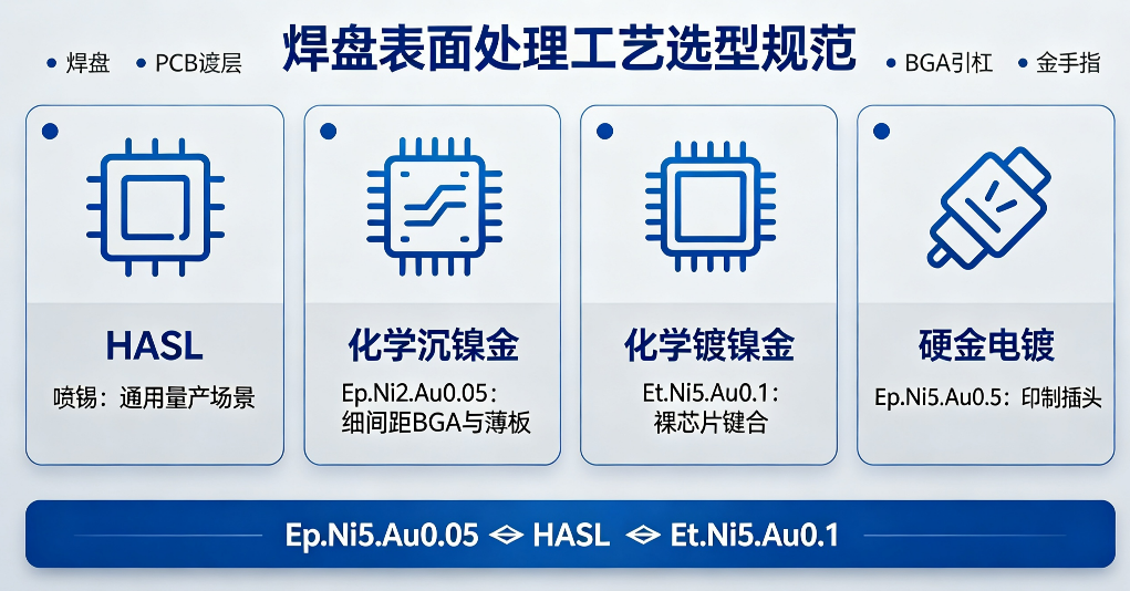
Based on high-frequency transmission characteristics, component package types, application scenarios, and cost control requirements, RF PCB pad surface finish processes are categorized into the following four standard solutions, each with specific application scenarios and technical requirements:
5.1 General Application Processes
For general-purpose RF PCBs, hot air solder leveling (HASL) with tin-lead alloy may be used, requiring a smooth tin surface free from exposed copper, oxidation, or pinholes, ensuring solderability for at least six months after board fabrication. To optimize high-frequency skin effect and reduce process-related contamination, electroless nickel immersion gold (ENIG) or organic solderability preservative (OSP) processes are preferred alternatives.
5.2 Fine-Pitch and Thin-Board Component Processes
For PCBs incorporating fine-pitch components such as 0.5 mm pitch BGAs or Rogers high-frequency boards with thickness ≤ 0.8 mm, electroless nickel immersion gold (process code: Ep.Ni2.Au0.05) is preferred. Conventional OSP processes suffer from short solderable shelf life, tacky surfaces, and poor tolerance to multiple reflow cycles, and are therefore not recommended for high-frequency RF PCB applications.
5.3 Bare Die and Keypad-Specific Processes
For bare dies requiring thermocompression or ultrasonic bonding (wire bonding processes), or RF mainboards integrating keypad structures, high-precision electroless nickel immersion gold (process code: Et.Ni5.Au0.1) must be used. For standard mass-produced products, full-board electroplated gold (process code: Ep.Ni5.Au0.05) may be employed. The Et.Ni5.Au0.1 process offers superior surface flatness, excellent thickness uniformity, and outstanding resistance to soldering heat, making it ideal for high-precision die bonding. The Ep.Ni5.Au0.05 full-board plating process is more cost-effective, with good surface consistency and brightness, suitable for standard volume production. In terms of cost comparison, high-precision electroless nickel immersion gold is more expensive than HASL, while full-board electroplated gold is less costly than HASL.
5.4 Printed Edge Connector-Specific Process
Printed edge connector areas on PCBs must use hard gold electroplating, with a nickel-cobalt doped gold alloy layer. Gold purity must be 99.5%–99.7%, standard plating thickness 0.5 μm–0.7 μm, and standard process code: Ep.Ni5.Au0.5.
The relationship between plating thickness and mating cycle life is standardized as follows: a 0.5 μm plating withstands 500 mating cycles, while a 1.0 μm plating withstands 1000 mating cycles. Selection should be based on product usage frequency and lifetime requirements.
6. High-Frequency PCB Fabrication Tolerance Control Requirements
The core control parameter for mass production of high-frequency RF PCBs is characteristic impedance accuracy, primarily influenced by the uniformity of resin content in the prepreg. Variations in lamination and forming process parameters among different PCB manufacturers can lead to inconsistent prepreg melt viscosity and cure degree, resulting in dielectric thickness deviations and ultimately causing dielectric constant shifts and impedance inaccuracies.
Therefore, to achieve high-precision mass production of high-frequency multilayer PCBs (including pure high-frequency laminates and hybrid high-frequency laminates), close process alignment between laminate suppliers and PCB manufacturers is essential. Resin content specifications, lamination profiles, and forming process parameters must be strictly harmonized to ensure stable dielectric properties and controllable impedance accuracy. Detailed process alignment standards are provided in Appendix C.
7. RF Component Selection and Soldering Process Requirements
7.1 Component Flatness and Packaging Requirements
The surface flatness tolerance of key RF components (such as ceramic-packaged modules including VCOs, power amplifiers, and filters) must be ≤ 0.005 inch to prevent poor component seating, which could lead to cold solder joints, voids, and abnormal signal transmission losses. During the R&D selection phase, new package types or alternative RF components must undergo early coordination with process engineering teams to complete manufacturability and solderability validation, thereby mitigating packaging compatibility risks.
7.2 Component Plating and Solder Joint Quality Requirements
Strict control must be maintained over the material and thickness of plating on RF component terminations. Silver-plated ceramic components are considered high-risk for soldering and are highly prone to voids, cold joints, and intermittent connections. During production, precise control of reflow temperature profiles, soak time, and environmental temperature/humidity is required to ensure reliable electrical and mechanical integrity of solder joints.
7.3 Component Electrical Tolerance Requirements
The electrical tolerance of RF passive components directly determines the overall performance consistency of RF circuits. Experimental validation shows that when component electrical tolerances exceed 5%, circuit distributed parameters become significantly dispersed, leading to degraded RF signal stability and poor batch-to-batch performance consistency. Therefore, during component selection, high-quality passive components with electrical tolerances ≤ 5% should be prioritized to ensure optimal circuit performance and manufacturing consistency.
7.4 RF Connector Technical Requirements
RF connector plating standards: center contact pins and digital signal pins must have a gold plating thickness of 30–50 μinch over a nickel underplate of 50–150 μinch. For SMT connectors, the dimensional tolerance at the contact interface with PCB pads must be tightly controlled to 0 to –0.002 inch to ensure tight contact, continuous impedance, and reliable connection, minimizing high-frequency contact loss and signal jitter.
8. Core Layout and Routing Guidelines for RF PCBs
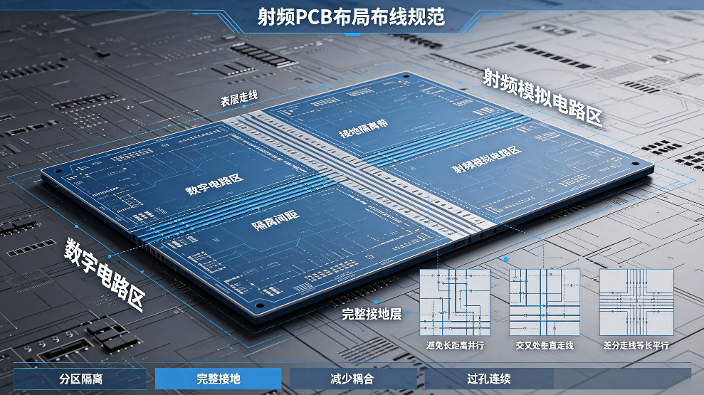
To suppress crosstalk between digital and RF analog signals, minimize signal loss and interference caused by capacitive and inductive coupling, and ensure high-frequency signal integrity, RF PCB layout and routing must strictly adhere to the following standardized guidelines:
Zonal Isolation Layout: Strictly separate digital circuit zones from RF analog circuit zones, maximize spacing between dissimilar circuit types, and prohibit digital traces from crossing into analog RF zones to fundamentally suppress inter-zone crosstalk.
Top-Layer Routing with Solid Ground Plane: Route RF signal traces preferentially on the PCB top layer, with a solid, unbroken, slot-free ground plane directly beneath to ensure complete grounding shielding, reducing radiated emissions and external interference coupling.
Crossing Trace Management: When RF traces unavoidably cross other signal lines, the optimal solution is to insert a grounded isolation strip between the two trace types, connected reliably to the main ground plane. As a secondary option, perpendicular cross-routing should be used to minimize coupling area and suppress capacitive interference.
Parallel Routing and Grounding Optimization: Avoid long parallel runs of RF traces whenever possible. If parallel routing is necessary, insert dedicated isolation ground traces between them, with evenly spaced vias to ground to maintain continuous shielding effectiveness. Surround individual RF traces with dense ground copper, connected to the main ground plane through vias.
Standardized Differential Pair Design: Implement RF differential pairs using equal-length parallel routing. Place grounded isolation traces along both outer edges of the pair, with evenly distributed ground vias along their entire length. Design the differential pair’s characteristic impedance strictly according to component specifications to ensure signal integrity and noise immunity.
trending news
Contact Us