



Sorry, no sales person is available right now to take your call. Pls leave a message and we will reply to you via email as soon as possible.
Home/ PCB News/ From Substrate to Finished Product: A Comprehensive Guide to the PCB Material Manufacturing Process
From Substrate to Finished Product: A Comprehensive Guide to the PCB Material Manufacturing Process
2026-06-18
Printed Circuit Boards (PCBs) serve as the core electrical interconnection platform in modern electronic devices, with their manufacturing processes deeply integrating technologies from materials science, fine chemicals, precision mechanical machining, and microelectronics fabrication. The performance foundation of a PCB lies in its Copper Clad Laminate (CCL) substrate—where the resin formulation system, composite reinforcement process, and hot-pressing quality collectively determine the board’s electrical characteristics, mechanical strength, thermal reliability, and service life. Industry production follows the fundamental principle of “substrate defines properties, processes impart functionality”: starting with CCL as the base material, PCBs are ultimately fabricated through refined backend processes—including pattern transfer, precision etching, drilling and metallization, multilayer lamination, and surface protection—to create finished boards capable of component mounting, signal transmission, and insulation protection.
This article systematically dissects the entire PCB manufacturing chain along the主线 of “CCL substrate preparation → precision PCB fabrication → differentiated processes for specialty substrates → industry technology trends,” providing in-depth explanations of core principles, critical parameters, and quality control points for each process step. It comprehensively covers both standard and specialty substrate technology systems, fully presenting the end-to-end technical logic—from raw materials to final PCB products.
1. Core PCB Substrate: Full Manufacturing Process of Copper Clad Laminate (CCL)
Copper Clad Laminate (CCL) is a functional base material formed by bonding reinforcement substrates, resin matrices, and copper foil under high temperature and pressure. It serves as the foundational substrate for rigid PCBs, flexible PCBs, and various specialty PCBs. Its complete production process comprises four core stages: resin varnish preparation, reinforcement impregnation, prepreg formation, and copper lamination with thermal curing. These stages are highly interdependent and sequential, collectively determining the laminate’s dielectric properties, thermal behavior, mechanical strength, and environmental stability.
1. Resin Varnish Preparation: Source Control of Substrate Performance
Resin varnish plays a dual critical role in binding the substrate and tuning functional properties. Its formulation and dispersion process are the origin of key CCL specifications—including dielectric constant (Dk), dissipation factor (Df), glass transition temperature (Tg), flammability rating, and coefficient of thermal expansion (CTE). To meet diverse application requirements in high-frequency communications, automotive electronics, industrial controls, and consumer devices, varnish formulations must be customized to precisely align material performance with end-use demands.
(1) Precise Raw Material Proportioning
The core varnish formulation consists of five components: base resin, curing agent, functional fillers, flame retardants, and organic solvents—all requiring precise metering and ratio control per process standards. Base resins may include epoxy, polyimide (PI), polytetrafluoroethylene (PTFE), or liquid crystal polymer (LCP). Dicyandiamide or imidazole-based curing agents precisely regulate crosslinking reaction rates to ensure uniform curing. Functional fillers such as silica, alumina, or hollow glass microspheres effectively reduce CTE, enhance thermal conductivity, and improve insulation stability. Flame retardants use halogen-free phosphorus-based or eco-friendly brominated systems to reliably achieve UL94 V-0 flammability ratings. Organic solvents like acetone or xylene adjust varnish viscosity to suit automated continuous impregnation processes.
Application Example: 5G millimeter-wave high-frequency CCLs employ low-Dk/Df PTFE resin systems combined with hollow glass microsphere fillers to significantly reduce high-frequency signal loss, meeting the demands of millimeter-wave high-speed communication. Standard FR-4 flame-retardant CCLs use modified brominated epoxy or halogen-free phosphorus-based formulations, balancing cost control with basic flame safety for mass-market consumer electronics.
(2) High-Speed Mixing and Dispersion
Base resin and organic solvent are loaded into a sealed reactor and thoroughly dissolved under constant temperature (50–80°C). Curing agents, functional fillers, and flame retardants are then sequentially added with precision. High-shear mixers (1000–3000 rpm) or ball mills perform fine dispersion to ensure uniform suspension of all fillers, eliminating local inhomogeneity and agglomeration. After dispersion, varnish viscosity is precisely adjusted to 1000–5000 cP to meet automated impregnation requirements.
(3) Filtration and Vacuum Deaeration
The prepared varnish passes through 100–200 mesh precision filters to remove undispersed filler agglomerates and mechanical impurities. It is then transferred to a vacuum deaeration unit, where microbubbles are removed under high vacuum (≤ -0.095 MPa), preventing pinholes, delamination, and voids in the final CCL and ensuring substrate density and performance uniformity.
2. Reinforcement Impregnation: Composite Bonding of Resin and Fibers
Reinforcement materials form the mechanical backbone of CCL, effectively suppressing board warpage, cracking, and flexural failure. The core objective of impregnation is to uniformly infiltrate, fill, and adhere resin into fiber interstices, creating a stable, homogeneous resin-fiber composite. Mainstream reinforcements include E-glass fabric, insulating paper, and synthetic nonwovens, with E-glass fabric being the preferred choice for mid-to-high-end CCLs due to its superior insulation and mechanical properties.
(1) Reinforcement Pre-Treatment
As-produced E-glass fabric contains starch-based sizing residues that significantly reduce resin-fiber interfacial adhesion. Therefore, dual pre-treatment—desizing and drying—is essential: sizing is removed via high-temperature calcination (200–300°C) or alkaline washing, followed by drying at 120–150°C to eliminate moisture that could cause curing bubbles or interlayer delamination. Paper-based materials used in economical grades like FR-1 require pre-impregnation with resin to enhance interfacial compatibility.
(2) Automated Impregnation and Pre-Curing
Pre-treated reinforcement moves continuously through an impregnation bath at 1–3 m/min for full resin saturation. Adjustable squeeze rollers precisely control resin pickup, typically 50–80% of the reinforcement’s dry weight. After impregnation, the material enters a drying oven (80–120°C) for 5–15 minutes to evaporate solvents and initiate partial crosslinking, forming prepreg. At this B-stage, the resin is non-tacky, flexible, and storable—ideal for subsequent lamination processes.
3. Lamination and Thermal Curing: Final CCL Formation
This stage is the core of CCL formation, where multiple prepreg layers are precisely stacked, bonded with copper foil, and fully cured under heat and pressure—transforming the resin from the B-stage to a rigid C-stage structure. This achieves monolithic integration of copper foil and insulating substrate. The industry-standard method is vacuum direct lamination.
(1) Precision Stack-Up Configuration
The number of prepreg layers is matched to target thickness—e.g., standard 1.6 mm FR-4 typically uses 4–6 layers. Electrodeposited copper foil (12–70 μm, for rigid PCBs) or rolled annealed copper foil (for flexible PCBs) is laminated onto both outer surfaces. Release films and stainless steel plates are placed on the outermost layers to prevent sticking and ensure uniform pressure distribution, guaranteeing flatness.
(2) Multi-Stage Thermal Curing
The stacked assembly is loaded into a vacuum press and cured using a segmented temperature-pressure profile to manage internal stress and avoid defects. The full cycle has three phases:
Ramp-up Phase: Gradually heat from room temperature to 120–150°C to melt and flow resin into fiber gaps, while pressure increases to 10–20 kg/cm²;
Curing Phase: Heat further to 170–190°C and hold for 1–2 hours to complete crosslinking, forming a dense, rigid insulating substrate;
Cool-down Phase: Cool naturally to below 80°C before depressurizing and unloading, preventing warpage or interlayer cracking from rapid cooling.
Key Quality Controls: Ramp rate ≤5°C/min to avoid thermal stress; uniform pressure across the panel to eliminate microvoids and ensure consistency.
(3) Post-Processing and Performance Testing
After curing, panels are trimmed to remove burrs, irregular edges, and stress-concentrated zones. Copper surfaces are finely polished to remove oxides and enhance adhesion for subsequent photoresist processes. Finished CCLs undergo sampling tests for dielectric properties, Tg, copper peel strength (industry standard ≥1.5 N/mm), and insulation resistance. Only batches meeting all specifications proceed to PCB fabrication.
2. PCB Fabrication: Precision Processing from CCL to Functional Circuit Board
CCL is merely an insulating base without circuit functionality. It must undergo a series of precision processes—including design preparation, pattern transfer, precision etching, drilling and metallization, multilayer lamination, surface finishing, and final inspection—to become a functional PCB capable of reliable electrical conduction, precise insulation, and secure component mounting.
1. Pre-Processing: Circuit Design and Phototool Generation
Based on end-product functional, structural, and electrical requirements, professional EDA software (e.g., Altium Designer, Cadence) is used to complete PCB layout, via design, pad placement, and stack-up planning, outputting standardized Gerber files. These files drive laser photoplotters to accurately replicate circuit patterns onto film negatives or dry films, creating high-precision masks for subsequent processing.
2. Pattern Transfer and Etching: Precision Formation of Conductive Traces
This process relies on photolithography, pattern development, and selective etching to retain functional copper traces while removing excess copper, forming circuits, pads, and conductive paths per design specs. It is critical to achieving trace accuracy and electrical consistency.
(1) Panel Surface Preparation
Specialized degreasers remove oils, dust, and contaminants from copper surfaces. Mild micro-etching with ammonium persulfate slightly roughens the copper to enhance photoresist adhesion. Multi-stage DI water rinsing and drying ensure a clean, dry, oxide-free surface for imaging.
(2) Photoresist Coating and Alignment Exposure
Liquid photoresist is uniformly coated, or dry film is laminated onto the panel under 100–120°C and 0.3–0.5 kg/cm². The photomask is aligned to the panel with high precision (alignment accuracy ≤0.02 mm) and exposed to 365 nm UV light. Exposed areas crosslink and harden; unexposed areas remain soluble, transferring the circuit pattern accurately.
(3) Development, Etching, and Stripping
A 1–2% sodium carbonate solution sprays the panel to dissolve unexposed resist, exposing copper for etching. The panel then moves at 1–2 m/min through an etchant bath (acidic cupric chloride or ferric chloride) at 40–50°C to remove exposed copper, leaving protected traces intact. After etching, sodium hydroxide strips the hardened resist, revealing clean copper circuits. Throughout, etch temperature, conveyor speed, and chemical concentration are tightly controlled to prevent undercutting, line-width variation, nicks, or pinholes.
3. Precision Drilling and Metallization: Enabling Interlayer Electrical Connection
Drilling and metallization are essential for multilayer PCBs to achieve interlayer conduction. Mechanical or laser drilling creates through-holes, blind vias, and buried vias, followed by metallization to ensure reliable electrical continuity. Processing accuracy directly impacts PCB reliability and yield.
(1) Precise Positioning and Drilling
Multilayer boards use X-ray alignment; single/double-sided boards use mechanical pins—keeping hole position error ≤0.02 mm. High-speed drills (30,000–100,000 rpm) with carbide bits (0.1–6 mm) are used. Aluminum entry sheets and phenolic backup boards minimize burrs, surface damage, and rough hole walls.
(2) Hole Cleaning and Metallization
Post-drilling, brush scrubbing and ultrasonic cleaning remove debris, dust, and oils from holes. Since hole walls are insulating, metallization is required: alkaline micro-etching activates the surface, followed by palladium chloride sensitization to form catalytic sites. Electroless copper deposits a 0.5–1 μm seed layer for initial conduction. Electrolytic copper plating then builds the layer to 5–20 μm, enhancing conductivity, adhesion, and mechanical reliability.
4. Multilayer Lamination: Integration of Multilayer PCBs
For 4+ layer PCBs, secondary lamination integrates inner layers. Inner layers are first etched per standard process, then black oxide treated to roughen copper and improve bonding with prepreg. Layers are precisely aligned per design stack-up and laminated using standard high-temperature, high-pressure profiles—ensuring no delamination, voids, or misregistration, and guaranteeing structural and electrical integrity.
5. Surface Finishing: Enhancing Solderability and Oxidation Resistance
Bare copper oxidizes easily, causing poor solder joints, opens, shorts, or insulation failure. Thus, surface finishing is mandatory after PCB fabrication. Mainstream finishes vary by application:
HASL (Hot Air Solder Leveling): Low cost, widely used, mature—common in general consumer electronics;
ENIG (Electroless Nickel Immersion Gold): Nickel blocks metal diffusion; gold enhances oxidation resistance and solderability—ideal for high-reliability, high-precision devices;
Immersion Silver: Excellent conductivity and minimal signal loss—optimized for high-frequency, high-speed applications;
OSP (Organic Solderability Preservative): Eco-friendly, cost-effective—forms a protective organic layer on copper, dominant in high-volume consumer electronics.
6. Solder Mask, Legend Printing, and Final Inspection
After surface finishing, green solder mask is screen-printed and cured to form an insulating protective layer, preventing shorts and solder bridging while enhancing environmental resistance, insulation stability, and lifespan. Component labels, part numbers, and fiducials are then printed for accurate assembly and maintenance.
Final electrical testing uses fixture-based or flying probe testers to detect shorts, opens, and insulation faults. AOI (Automated Optical Inspection) and manual review identify visual defects like nicks, burrs, or misalignment. Qualified boards are routed or laser-cut to final dimensions, completing the PCB fabrication process.
3. Process Differentiation in Specialty PCB Materials
Beyond standard rigid FR-4, specialty PCBs—such as Flexible PCBs (FPCs), ceramic-based PCBs, and metal-core PCBs—are engineered for extreme conditions like repeated flexing, high thermal conductivity, high-temperature operation, low-loss high-frequency transmission, and high-power handling. They feature differentiated processes in substrate selection, surface treatment, lamination, and post-processing to meet stringent application demands.
1. Key Process Features of Flexible PCBs (FPCs)
FPCs use polyimide (PI) film as the base, offering ultra-thin, lightweight, and highly flexible characteristics—ideal for wearables, foldable devices, and precision modules. Process differences focus on interface treatment and forming:
Substrate Activation: PI’s smooth, low-energy surface requires plasma or alkaline etching to roughen and activate it, ensuring strong copper adhesion and flex reliability.
Differentiated Copper Lamination: Highly ductile rolled copper is preferred, laminated at 200–250°C under 5–10 kg/cm². Alternatively, electroless copper can form flexible conductive layers for dynamic flexing applications.
Flexible Protection: Rigid solder mask is replaced by PI coverlay, thermally bonded to provide insulation and withstand repeated bending without cracking.
Reliability Validation: Finished FPCs must survive >10,000 cycles of 180° bending without trace fracture, delamination, or performance degradation.
2. Key Process Features of Ceramic-Based PCBs
Ceramic PCBs use alumina (Al₂O₃) or aluminum nitride (AlN) substrates, offering exceptional thermal stability, high thermal conductivity, low CTE, and superior insulation—used in power semiconductors, high-end LED packaging, aerospace, and high-voltage controls. Six mature process technologies exist, each with distinct advantages:
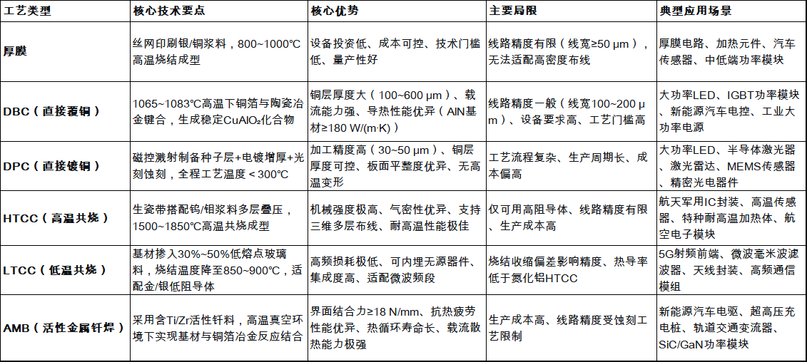
Process Selection Guidelines: Ultra-high wiring precision favors DPC; high-frequency integration prefers LTCC; ultra-high power/reliability uses AMB; high-current/moderate precision selects DBC; low-cost consumer applications choose thick-film; extreme high-temp/hermetic military needs HTCC—covering all high-end application scenarios.
3. Key Process Features of Metal-Core PCBs
Metal-core PCBs use aluminum or copper bases for superior heat dissipation, solving thermal challenges in high-power applications like LED lighting, industrial power supplies, EV controls, and motor drives. Process differentiation centers on insulation layer formation and lamination:
Custom Insulation Layer: A modified epoxy resin filled with ceramic thermal conductors is coated onto the metal base (50–200 μm thick) and cured at 150–180°C, achieving dielectric strength ≥2 kV while enabling efficient heat transfer.
Precision Low-Pressure Lamination: Copper foil is bonded at 160–180°C under 3–5 kg/cm², achieving peel strength ≥1.0 N/mm while avoiding metal deformation or insulation cracking from excessive heat/pressure.
4. Key Trends in Modern PCB Manufacturing
Rapid advancements in 5G mmWave, AI, data centers, EVs, and smart devices are driving electronics toward higher frequencies, greater miniaturization, higher power density, and greener manufacturing—pushing PCB materials and processes to continuously evolve.
1. Deep Iteration of High-Frequency/High-Speed Processes
To meet low-loss mmWave signal transmission needs, the industry is optimizing lamination profiles (temperature, pressure, ramp rate) for low-Dk/Df materials like PTFE and LCP—precisely controlling dielectric loss and residual stress to mitigate signal delay, attenuation, and crosstalk in 5G base stations, automotive radar, servers, and chip substrates.
2. Continuous Breakthroughs in High-Density Integration
Any-layer interconnect (ALIVH), micro-vias (≤0.1 mm), and ultra-fine-line processes are scaling up, with mainstream capabilities now achieving ≤20/20 μm line/space—key for advanced HDI, IC substrates, and Chiplet packaging, aligning with device trends toward thinner, smaller, and more integrated designs.
3. Universal Adoption of Green and Low-Carbon Processes
The industry is phasing out lead plating and brominated flame retardants, promoting halogen-free substrates, OSP finishing, water-based solder masks, and low-temperature curing—fully complying with RoHS, REACH, and other global environmental standards to enable harmless, low-carbon PCB lifecycles and sustainable growth.
5. Conclusion
PCB manufacturing is a systematic engineering discipline spanning molecular formulation, mesoscale composite forming, and macro-scale precision processing. CCL formulation, filler engineering, and lamination fundamentally define a PCB’s electrical, mechanical, and thermal performance. Backend processes—including pattern transfer, precision drilling, metallization, lamination, and surface finishing—impart stable electrical functionality and long-term reliability. Meanwhile, differentiated processes for flexible, ceramic, and metal-core PCBs fill critical gaps in extreme environments—enabling full-scenario adaptability.
Driven by rapid electronics innovation, PCB manufacturing is accelerating toward higher precision, better performance, greater reliability, and greener practices. As a foundational enabler of the information age, continuous PCB process breakthroughs will keep empowering cutting-edge fields—from 5G and EVs to AI, advanced manufacturing, and semiconductor packaging.
trending news
Contact Us