



Sorry, no sales person is available right now to take your call. Pls leave a message and we will reply to you via email as soon as possible.
Home/ PCB News/ High-Frequency / High-Speed PCB Substrate Selection: FR-4, Rogers, Megtron
High-Frequency / High-Speed PCB Substrate Selection: FR-4, Rogers, Megtron
2026-05-27
With the widespread adoption of technologies such as PCIe 5.0/6.0, 77GHz millimeter-wave radar, 5G RF, and PAM4 high-speed optical modules, PCB substrate materials directly determine signal integrity and mass production yield. Mismatched substrates can easily cause excessive signal loss, impedance deviation, delamination, and board warpage. This article collaborates with the Baineng Yunban process R&D team to provide hardware, RF, and SI engineers with an in-depth breakdown of three mainstream substrate families—FR-4, Rogers, and Megtron—combining real-world test data and mass production experience to deliver a complete material selection guide, process recommendations, and acceptance criteria, enabling engineers to rapidly implement cost-effective and manufacturable substrate choices.
The following sections compare the electrical performance, advantages/disadvantages, process complexity, and application scenarios of these three substrate types. Additionally, leveraging Baineng Yunban's high-frequency/high-speed PCB mass production cases, we supplement the discussion with a material selection decision matrix and mandatory pre-production inspection standards, offering a one-stop solution to high-speed/high-frequency PCB material selection challenges.
1. Fundamental Core Concepts
To establish a unified evaluation benchmark for engineers to cross-compare substrate performance, all electrical parameter measurements referenced below are standardized under the following conditions: 10 GHz frequency, 25°C ambient temperature, and dry, non-hygroscopic environment. The definitions of two key dielectric parameters are explained as follows:
Dk (Dielectric Constant): A critical parameter governing transmission line characteristic impedance and signal phase delay. In high-frequency/high-speed designs, Dk must not only be low in value but also exhibit minimal sensitivity to frequency and temperature variations. Smaller Dk fluctuations reduce impedance matching difficulty and effectively prevent signal reflection and phase shift issues.
tanδ (Dissipation Factor): Represents the inherent attenuation of alternating signals by the dielectric material and is the top-priority metric in high-frequency/high-speed substrate selection. A lower tanδ value means less heat-induced signal loss within the dielectric, providing greater tolerance margins for high-frequency, high-data-rate transmission links.
2. Overview of Key Parameters for Mainstream Substrates
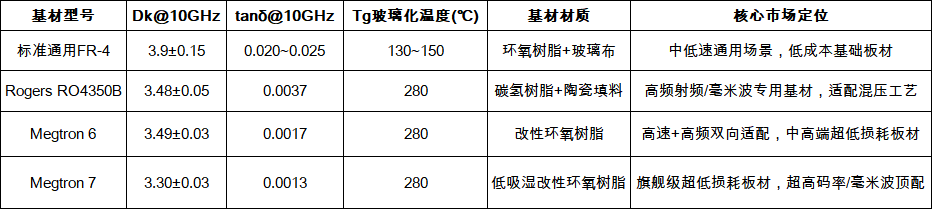
The table below summarizes core parameters for four widely used engineering substrates: standard FR-4, Rogers RO4350B, and Sumitomo Megtron 6/7, covering electrical performance, thermal resistance, material composition, and market positioning, clearly delineating performance tiers and application ranges:
3. In-Depth Analysis and Engineering Recommendations for Substrate Types
3.1 Standard FR-4: Cost-Effective General-Purpose Substrate with Performance Limits in High-Frequency/High-Speed Applications
Key Advantages
Outstanding Cost Efficiency: Compared to high-end specialty substrates like Rogers and Megtron, total material costs can be reduced by 60%–80%, and mature manufacturing processes enable immediate mass production with minimal investment;
Global Supply Chain Coverage: As the industry-standard base material, it is producible by the vast majority of PCB manufacturers worldwide, ensuring ample procurement channels and no supply bottlenecks;
Strong Process Compatibility: Fully mature processes for lamination, drilling, etching, and surface finishing ensure stable mass production yields and simplify troubleshooting of downstream process anomalies.
Performance Limitations
High Dielectric Loss: At 10 GHz, tanδ can reach up to 0.025, corresponding to an insertion loss of approximately 0.35 dB/inch—resulting in significant signal attenuation under high-frequency operation;
High Sensitivity to Temperature and Frequency: Dk values fluctuate significantly with frequency and environmental temperature/humidity, making precise impedance control difficult in high-frequency links and prone to signal reflection and resonance;
Limited Thermal Resistance: Glass transition temperature (Tg) is only 130–150°C, insufficient to withstand multiple high-temperature reflow cycles, leading to board warpage and layer misalignment during multilayer fabrication and SMT processes.
Application Boundaries
This substrate is suitable only for signal links with operating frequencies ≤10 GHz and per-channel data rates ≤16 Gbps. Typical applications include passive layers in 3.5 GHz 5G AAUs, consumer electronics mainboards, industrial control PCBs, power supply boards, and low-speed communication backplanes. It is strictly prohibited for use in millimeter-wave bands or high-demand scenarios such as PCIe 4.0+ high-speed serial buses.
3.2 Rogers RO4350B: Benchmark for Cost-Effective Mass Production in High-Frequency Millimeter-Wave Applications
Key Advantages
Low-Loss at High Frequencies: At 10 GHz, tanδ is 0.0037—over six times lower than standard FR-4—significantly reducing RF signal attenuation;
Exceptional Electrical Stability: Across the ultra-wide 1–40 GHz RF band, Dk variation is less than 0.02 with minimal influence from temperature and humidity, perfectly meeting the stringent impedance-matching requirements of RF circuits;
Superior High-Temperature Resistance: Tg reaches 280°C, enabling endurance of multiple high-temperature reflow cycles and compatibility with complex multilayer hybrid stack-up processes.
Engineering Challenges
Poor CTE (Coefficient of Thermal Expansion) match with standard FR-4: RO4350B has a Z-axis CTE of 45 ppm/°C, while conventional FR-4 exhibits a much higher Z-axis CTE of ~250 ppm/°C. Direct hybrid lamination of these two materials creates unreleased thermal stress during thermal cycling, easily causing interlayer delamination, substrate cracking, and layer misalignment—severely reducing mass production yield.
Mass Production Optimization Strategies
Interlayer Stress Buffering: Insert a 10–15 μm polyimide buffer film between the Rogers high-frequency layer and FR-4 base layer to compensate for CTE mismatch and relieve interlayer thermal stress;
Advanced Imaging Process: Adopt LDI (Laser Direct Imaging) technology to control trace alignment tolerance within ±15 μm, mitigating layer misalignment in hybrid stack-ups;
Customized Lamination Profile: Use a low-temperature pre-press followed by staged high-temperature curing to accommodate the distinct thermal shrinkage behaviors of both materials and reduce delamination risk.
Target Applications
Ideal for 20–80 GHz millimeter-wave bands and pure RF signal paths. Typical uses include 77 GHz automotive radar, 5G base station and terminal RF front-ends, RF layers in mid-to-low-speed optical modules, and satellite communication high-frequency dedicated PCBs.
3.3 Sumitomo Megtron 6/7: Flagship Substrate for Dual High-Speed + Millimeter-Wave Scenarios
The Megtron series, developed by Sumitomo Electric, consists of modified epoxy-based ultra-low-loss laminates. Unlike Rogers materials optimized primarily for RF/high-frequency applications, Megtron simultaneously satisfies the transmission demands of both high-speed digital and high-frequency RF signals, making it the preferred choice for premium high-speed PCB projects.
Key Performance Highlights
Industry-Leading Low Loss: Megtron 6 achieves tanδ as low as 0.0017, while flagship Megtron 7 reaches just 0.0013—65% lower loss than RO4350B—placing its broadband attenuation performance at the forefront of the industry;
Excellent Environmental Robustness: Moisture absorption is only 0.12%, ensuring negligible drift in Dk and tanδ under high-humidity or thermal cycling conditions, eliminating signal distortion and impedance shifts caused by humidity;
Superior Millimeter-Wave Performance: At 80 GHz, phase delay variation is only ±0.8°/inch—far better than RO4350B’s ±2.3°/inch—effectively resolving phase mismatch issues in millimeter-wave systems.
Processing Challenges and Process Requirements
Megtron series imposes extremely high demands on PCB manufacturers’ equipment precision and process expertise, making mass production unfeasible for smaller vendors. Key process constraints include:
Lamination Process: Must employ a customized multi-stage ramp-up profile (170°C → 220°C → 270°C) to gradually release internal stresses and prevent warpage or delamination;
Drilling Process: Requires specialized diamond-coated drill bits with spindle speed fixed at 120 kRPM to minimize via wall roughness and reduce additional signal loss from via structures;
Cost Disadvantage: High raw material costs, coupled with expensive equipment, stringent process controls, and skilled labor, result in significantly higher total production costs compared to FR-4 or Rogers hybrid solutions.
Target Applications
Designed for cutting-edge R&D scenarios requiring ultra-high data rates and operating frequencies. Typical applications include PAM4 optical modules at 28 Gbps+, PCIe 5.0/6.0 server motherboards, 80 GHz+ phased-array radar, and high-end AI computing high-speed backplanes.
4. Standardized Material Selection Decision Matrix
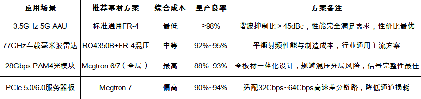
Based on four core decision factors—operating frequency, data rate, production cost, and yield—we recommend optimal substrate solutions for mainstream industry applications and annotate key characteristics to help R&D teams balance project budgets against performance requirements:
5. Mandatory Validation Tests for Mass Production (Hard Acceptance Criteria)
After finalizing the substrate type and stack-up design, the following three validation tests must be completed before full-scale production to proactively identify design and process risks and avoid mass scrap. All tests must be conducted using the actual production stack-up structure and process parameters:
5.1 TDR Impedance Consistency Test
Acceptance Criteria: Characteristic impedance tolerance for single-ended/differential traces ≤ ±5%. Focus on vulnerable structures such as stub vias, layer-transition vias, trace corners, and branch lines. For high-frequency/high-speed specialty substrates, repeat testing after thermal cycling is required to verify impedance stability.
5.2 Wide-Temperature Eye Diagram Integrity Test
Test Range: Full operational temperature range from -40°C to 85°C. Acceptance Criteria: Eye height degradation for PAM4/NRZ signals ≤ 30%, with no eye closure or jitter exceeding thresholds throughout, validating signal transmission stability under complex thermal conditions.
5.3 Reflow Warpage Measurement
Test Protocol: Use a standard 200×200 mm test coupon replicating the production reflow profile. Acceptance Criteria: Total Z-axis board deformation < 0.3 mm to prevent SMT assembly defects such as solder voids, component misalignment, or chip fractures.
6. Summary and Core Selection Principles
FR-4: Suitable for general-purpose projects below 10 GHz and 16 Gbps, offering low cost and ease of mass production as core advantages. Not recommended for advanced high-frequency/high-speed applications;
Rogers RO4350B: The optimal solution for 20–80 GHz millimeter-wave and pure RF links. When combined with buffer layers and specialized hybrid lamination processes, it delivers the best balance of performance and cost for RF products;
Megtron 6/7: The performance ceiling for integrated high-speed digital (>28 Gbps) and millimeter-wave applications, exclusively designed for flagship products such as PCIe 6.0, premium optical modules, and phased-array radar.
Core Principle of Substrate Selection: There is no universal "best" PCB substrate—only the optimal solution tailored to specific project requirements. Engineers must holistically evaluate five dimensions: operating frequency, signal data rate, environmental temperature/humidity, production budget, and the PCB manufacturer’s process capabilities. Early alignment with the PCB vendor on stack-up design, lamination profiles, drilling parameters, and other details is essential to prevent signal integrity issues and mass production failures at the design stage.
Baineng Yunban Implementation Guidance: Addressing the mass production pain points of different substrate tiers, Baineng Yunban leverages its mature high-speed/high-frequency PCB smart manufacturing line to offer end-to-end support. For standard FR-4, the platform enables rapid prototyping and scalable volume production, ideal for cost-sensitive consumer electronics and industrial control projects. For Rogers hybrid laminates, customized buffer-layer stack-ups and high-precision LDI processes are provided to resolve common issues like delamination and layer misalignment in millimeter-wave radar boards. For premium ultra-low-loss Megtron 6/7 substrates, dedicated advanced lamination equipment and diamond-drilling process teams support high-specification production for PCIe 6.0 and high-speed optical modules. Additionally, engineers can upload stack-up files directly on the Baineng Yunban platform to receive integrated services—including SI loss prediction, DFM (Design for Manufacturability) review, and cost quoting—significantly accelerating the selection-to-production cycle.
trending news
Contact Us