



Sorry, no sales person is available right now to take your call. Pls leave a message and we will reply to you via email as soon as possible.
Home/ PCB News/ Baineng Yunban 16-Layer 2-Stage HDI Industrial Vision Motherboard: A Benchmark for High-Density Interconnect and Industrial Reliability
Baineng Yunban 16-Layer 2-Stage HDI Industrial Vision Motherboard: A Benchmark for High-Density Interconnect and Industrial Reliability
2026-06-02
With the iterative advancement of industrial automation, machine vision, and edge AI technologies, high-definition imaging, high-frame-rate data acquisition, and high-density computing integration have become core development trends for industrial inspection equipment. Against this industry backdrop, the core PCB motherboard—serving as the carrier for signal transmission, power distribution, and chip integration—has made signal integrity, power integrity, routing density, and long-term reliability under all operating conditions critical factors limiting the performance ceiling of high-end industrial equipment.
Addressing pain points in high-performance industrial vision, high-speed signal processing, and edge computing applications, BaiNeng YunBan has launched a 16-layer, 2-stack HDI motherboard specifically designed for industrial vision systems. Integrating second-order laser blind/buried via interconnect technology, high-Tg anti-aging specialty substrate materials, and micron-level precision manufacturing, the product achieves breakthroughs in routing density, high-frequency signal transmission, and wide-temperature environmental adaptability. It effectively balances the performance and manufacturing cost of advanced HDI solutions, delivering a high-value, highly stable PCB integrated solution for mid-to-high-end industrial intelligent devices.
1. Core Technical Specifications
This product is professionally optimized across multiple dimensions—including lamination structure, substrate selection, via/pad size, trace width, and surface finish—to fully align with the application demands of industrial vision equipment: high-density integration, high-speed transmission, and 24/7 operation. Detailed technical parameters and industry value are as follows:
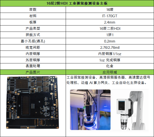
Product Technical Positioning – Comparative Analysis
To precisely match customer selection requirements at different tiers, the table below provides a comprehensive comparison among this product, conventional multilayer boards, and advanced 3-stack HDI boards across dimensions such as lamination structure, fabrication precision, fan-out capability, signal performance, and overall cost—clearly defining its ideal application scenarios and differentiated advantages:
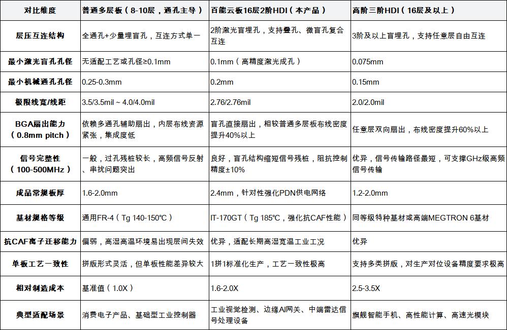
Selection Guidance: For mid-to-high-end industrial equipment requiring significantly higher routing density, signal integrity, and environmental reliability than traditional multilayer boards—but not needing the ultra-high precision of 3-stack HDI processes while aiming to control hardware costs—this 16-layer, 2-stack HDI motherboard offers the optimal cost-performance ratio.
In-Depth Analysis of Core Technical Advantages
Second-Order HDI Interconnect Technology: Co-Optimization of High-Density Integration and High-Frequency Signal Performance
The product employs a dual-stage laser blind/buried via lamination process, combining stacked blind vias with micro-blind via hybrid interconnect technology to fundamentally resolve fan-out challenges for high-pin-count BGA chips. Compared to traditional through-hole multilayer boards, routing density increases by over 40%, enabling efficient parallel integration of multiple FPGAs and AI inference chips.
Moreover, the short-path blind via structure significantly reduces stub length, minimizing reflection loss and crosstalk during high-frequency signal transmission. Within the 100–500 MHz mid-to-high frequency range, signal integrity metrics comprehensively outperform conventional PCB solutions, making it ideally suited for interfaces such as Camera Link, MIPI, and high-speed differential buses—providing stable signal transmission support for high-definition image capture, high-speed radar data processing, and real-time inference workloads.
IT-170GT Specialty Substrate: Foundational Guarantee for Industrial-Grade, All-Weather Reliability
The motherboard utilizes ITEQ’s custom IT-170GT halogen-free, high-Tg copper-clad laminate, featuring a glass transition temperature (Tg) of up to 185°C and a thermal decomposition temperature exceeding 335°C. This provides ample thermal safety margin for lead-free SMT reflow soldering, wave soldering, and other assembly processes, effectively preventing delamination and warpage caused by high-temperature fabrication.
Additionally, this substrate offers two key properties: low coefficient of thermal expansion (CTE) and exceptional resistance to Conductive Anodic Filament (CAF) ion migration. It withstands harsh industrial conditions—including rapid temperature swings, high humidity, and dust—maintaining long-term interlayer insulation and mechanical stability. This material-level enhancement reduces failure risks such as substrate aging, interlayer short circuits, and insulation breakdown, supporting 24/7 continuous operation.
Micron-Level Precision Manufacturing: End-to-End Process Accuracy Control
Leveraging BaiNeng YunBan’s mature large-scale second-order HDI manufacturing system, the product achieves precision control across all fabrication stages: via formation tolerance is maintained within 5%, and layer-to-layer alignment accuracy reaches ±25μm. Vacuum-integrated lamination combined with full-spectrum X-ray non-destructive testing completely eliminates internal defects such as voids, layer misalignment, or registration errors—preventing short circuits and open circuits.
Furthermore, the factory has achieved stable mass production capability for ultra-fine traces as narrow as 2.76 mil (line/space), enabling precise implementation of high-speed differential pair length matching, ground shielding, and impedance control—meeting the stringent technical standards of high-end industrial equipment for high-density routing and high-precision impedance management.
ENIG (Electroless Nickel Immersion Gold) Surface Finish: Long-Term Assembly and Contact Reliability
The board surface uniformly adopts ENIG surface treatment, forming a homogeneous plating structure with a 5μm nickel layer and a 0.05–0.1μm gold layer. This coating delivers excellent solderability, oxidation resistance, and wear durability—not only supporting fine-pitch component assembly with reduced risk of cold or missed solder joints, but also maintaining stable low contact resistance over time. It withstands frequent plugging/unplugging and high-vibration industrial environments, preventing equipment downtime caused by connector oxidation or poor contact.
Detailed Application Scenarios
Industrial Vision Inspection Equipment (Lithium Battery / 3C / Semiconductor Industries)
Scenario Overview
Taking an online defect inspection project for electrode coating from a leading lithium battery equipment manufacturer as an example: the system integrates four 20-megapixel line-scan cameras (Camera Link, 85MHz clock) and one high-end Xilinx Zynq UltraScale+ FPGA with ~900 BGA pins, along with a 6-axis servo motion control system. The equipment must operate continuously in a 0–50°C production environment, with an industry-mandated false detection rate below 0.05%.
Industry Pain Points
High-pin-count BGA fan-out is extremely challenging: traditional through-hole designs compromise power plane integrity and consume excessive inner-layer routing resources, failing to meet high-density integration needs;
Stringent high-speed differential signal control: Camera Link signals run at 850 Mbps, requiring intra-pair skew <5 ps and characteristic impedance stabilized at 100Ω ±10%;
Significant power and thermal management pressure: the FPGA draws instantaneous core current up to 15A, and DDR4 memory requires low-noise, stable power;
High reliability demands: long-term exposure to vibration and temperature fluctuations on production lines can cause solder joint cracking and connector contact failures.
Customized Solution
Lamination Structure Optimization: Layers L1/L16 carry Camera Link and MIPI high-speed signals; L2/L15 are dedicated full-coverage ground planes for signal shielding; L3/L14 serve as independent power layers, with localized 2oz thickened copper reducing DC resistance by 50% to enhance high-current delivery; L4–L13 are reserved for inner-layer signals and low-speed control. Combined with a second-order hybrid blind via structure, this design separately addresses high-speed signal fan-out, direct chip power connections, and short-path memory interconnects. Post-optimization, BGA fan-out density increased by 45%, signal paths shortened by 30%, and via stub effects were entirely eliminated.
High-Speed Signal Optimization: All high-speed differential pairs are routed on outer layers with a solid underlying ground reference. Uniform 2.76 mil trace/space yields measured impedance between 99.2Ω and 101.5Ω, meeting the tight 100Ω ±8% control standard. Ground shielding traces and stitching vias between differential pairs achieve crosstalk suppression better than -40dB. Eye diagram results: at 85MHz clock frequency, eye height >600mV, eye width >0.7UI, and jitter <50ps—reaching industry-leading performance.
Power Integrity Optimization: Under the FPGA, a PDN network is built using 16 × 330μF tantalum capacitors and 32 × 0.1μF X7R MLCC high-frequency capacitors. Second-order blind vias shorten capacitor grounding loops to under 1mm, achieving PDN impedance <5mΩ across the 1MHz–100MHz spectrum.
Reliability Validation: IT-170GT substrate passed 1,000-hour high-temperature/high-humidity (50°C, 90% RH) CAF aging test with no ion migration; ENIG connectors endured 500 insertion cycles with contact resistance variation <2mΩ; the board passed IEC 60068-2-64 vibration testing and 300 thermal cycles (-20°C to 70°C) with no delamination, solder cracks, or impedance shift >3%.
Customer Benefits
Board integration density significantly improved, reducing overall equipment volume by 25%; compared to 3-stack HDI solutions, hardware BOM cost was directly reduced by 30%; after 18 months of deployment, zero PCB-related failures occurred, false detection rate dropped to 0.02%, and overall inspection yield rose to 99.95%. This solution has now been platformized and reused across multiple vision systems, including 3C glass cover inspection and semiconductor packaging AOI.
High-Definition Video Servers (Industrial Security / Intelligent Surveillance)
Scenario Challenges:Multi-channel 4K/8K video servers face insufficient BGA fan-out space for codec chips, DDR4 signal distortion, and excessive power noise under high load—leading to video stuttering and poor system stability.
Solution:Leveraging the 16-layer stackup, dedicated routing layers are allocated for memory buses and video differential signals to achieve precise impedance matching; second-order HDI optimizes BGA fan-out and shortens signal paths; 2.4mm board thickness strengthens the PDN network to support stable operation of multiple high-power chips.
Implementation Results:Stably supports 16+ channels of HD video streams; equipment MTBF exceeds 100,000 hours.
High-Speed Radar Signal Processors (Industrial Inspection / Millimeter-Wave Radar)
Scenario Challenges:Equipment must process GHz-level signals, suffering from high transmission loss and significant crosstalk; dielectric constant drift of substrates under wide-temperature conditions causes signal distortion, degrading detection accuracy.
Solution:IT-170GT substrate offers low dielectric constant, low loss, and stable electrical parameters—reducing high-frequency signal attenuation; multi-layer partitioned routing isolates acquisition, computation, and power lines to suppress crosstalk; high-Tg substrate ensures stable dielectric properties across wide temperature ranges.
Implementation Results:Ensures radar signal fidelity, enabling millimeter-level non-contact inspection in industrial settings.
Edge AI Compute Gateways (Industrial IoT / Smart Manufacturing)
Scenario Challenges:AI gateways integrate multiple compute chips and industrial interfaces, leading to inadequate chip cooling; limited PCB space for ESD protection circuits; high humidity, dust, and vibration in workshops increase failure rates.
Solution:2.4mm board thickness incorporates thermal via arrays to enhance chip heat dissipation; second-order HDI frees up surface space for optimized ESD layout on Ethernet and RS485 interfaces; high-reliability substrate + ENIG finish ensures robustness in harsh production environments.
Implementation Results:Edge inference latency controlled to milliseconds; equipment operates reliably under complex conditions over extended periods.
High-End Automation Master Controllers (PLC / Multi-Axis Motion Control)
Scenario Challenges:High-end PLCs and motion control cards feature dense routing, where electromagnetic interference (EMI) can trigger false signals; long-term operation risks interlayer insulation failure and connector contact degradation, reducing control precision.
Solution:16-layer partitioned routing separates control signals, buses, and power lines; differential shielding and impedance control enhance EMI immunity; CAF-resistant substrate prevents interlayer failure, and ENIG finish ensures long-term connector reliability.
Implementation Results:Effectively eliminates EMI-induced malfunctions; multi-axis synchronization error controlled within ±1μm.
Technical Support and Quality Assurance
BaiNeng YunBan has deep expertise in R&D and large-scale production of advanced HDI PCBs and high-multilayer specialty circuit boards, backed by a mature system encompassing process development, manufacturing control, and post-sales enablement—fully capable of meeting customized industrial client requirements.
For this 16-layer, 2-stack HDI industrial vision motherboard, we offer end-to-end value-added services including Gerber review, DFM manufacturability optimization, custom impedance modeling, stackup design, and specialized reliability testing. We support flexible delivery—from small-batch prototyping to high-volume production—with full-process tracking of fabrication progress and quality inspection.
Spanning industrial automation, machine vision, edge AI, high-speed radar, and intelligent security, BaiNeng YunBan remains committed to delivering PCB products characterized by high density, high reliability, and high performance—empowering downstream clients to enhance equipment capabilities and reduce R&D and production costs, jointly building an ecosystem for high-end industrial intelligence. For detailed stackup proposals, test reports, or customized adaptation services, please contact our technical team at any time.
trending news
Contact Us