

Sorry, no sales person is available right now to take your call. Pls leave a message and we will reply to you via email as soon as possible.
Home/ PCB News/ PCB Embedded Capacitance Empowers PDN Optimization for High-Power AI Accelerators
PCB Embedded Capacitance Empowers PDN Optimization for High-Power AI Accelerators
2026-05-22
In the conventional understanding of the PCB industry, multilayer boards are predominantly structured with even-numbered layers such as 2, 4, 6, and 8. However, odd-layer PCBs are not nonexistent—they exist exclusively within the HDI (High-Density Interconnect) board system, accounting for approximately 5% of the market share. The fundamental distinction between these two product types lies in their stack-up logic: standard even-layer HDI boards employ a core-based design, whereas niche odd-layer HDI boards rely entirely on a coreless process architecture.
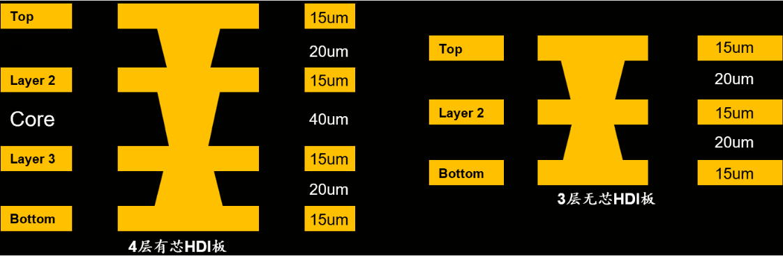
Even-layer HDI boards use traditional core substrates as their structural foundation, representing the most mature and widely adopted solution in the industry. In contrast, odd-layer HDI boards completely eliminate the core substrate, achieving differentiated performance through coreless technology. This article will systematically analyze the technical boundaries and application scenarios of core-based versus coreless HDI from perspectives including stack-up structure, manufacturing processes, thickness limits, comparative advantages and disadvantages, and market applications.
I. Stack-Up Differences: Structural Framework Determines Fundamental Characteristics
The essential difference between core-based and coreless HDI lies in whether they incorporate a solid core substrate that provides mechanical support, electrical insulation, and serves as an electrical reference plane. This foundational distinction subsequently leads to significant divergences in performance, manufacturing processes, and reliability.
1. Core-Based HDI Structure
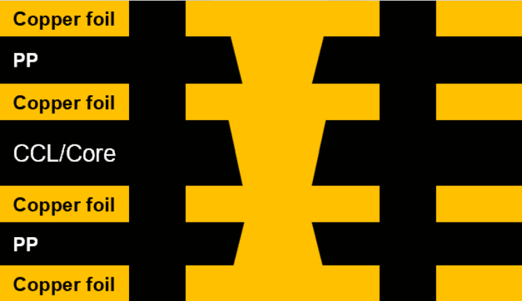
Core-based HDI boards retain the core architecture of traditional multilayer PCBs, using a pre-patterned copper-clad laminate (CCL) core as the board’s "rigid skeleton." This core serves dual roles as both a mechanical foundation and an electrical reference layer. Building upon this base, sequential buildup layers with microvias are formed by laminating prepreg (PP) as the insulating bonding medium onto one or both sides of the core, ultimately creating a high-density interconnect multilayer structure.
A typical symmetric stack-up is: copper foil–PP–core–PP–copper foil. This symmetric design effectively counteracts lamination stress, providing excellent structural stability and resistance to warpage—key reasons for the high yield and dimensional stability of core-based boards, which naturally align with even-layer stacking logic.
2. Coreless HDI Structure
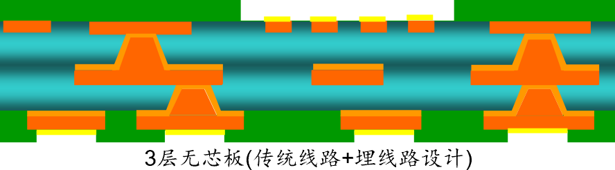
Coreless HDI boards completely eliminate the solid core substrate, instead using ultra-thin insulating materials such as prepreg (PP) or ABF as the base. Circuit layers are built up sequentially through lamination without any rigid skeletal support.
This structure breaks the traditional limitation that core-based designs can only achieve even-numbered layers, enabling flexible designs such as 3-layer or 5-layer odd-layer HDI. Moreover, by eliminating the thick core substrate, coreless boards achieve extreme thinness, making them a critical technological pathway for ultra-thin, high-end PCBs.
II. Process Comparison: Mature Continuity vs. Innovative Breakthrough
1. Core-Based HDI: Mature Processes with Excellent Compatibility
The manufacturing process for core-based HDI boards is an extension and enhancement of traditional multilayer PCB fabrication, inheriting a mature technological framework with strong compatibility to existing production lines. The overall workflow closely aligns with standard multilayer board processes, enabling mass production without major equipment modifications—resulting in low investment costs, minimal risk, and high process controllability. Consequently, it remains the dominant choice for PCB manufacturers worldwide.
For interlayer interconnects, core-based boards leverage well-established techniques such as mechanical drilling, laser drilling, and vertical plating/filling, backed by deep technical expertise and stable yields sufficient to meet mid-to-high-end precision interconnect requirements.
2. Coreless HDI: Carrier-Assisted, Complex Processes
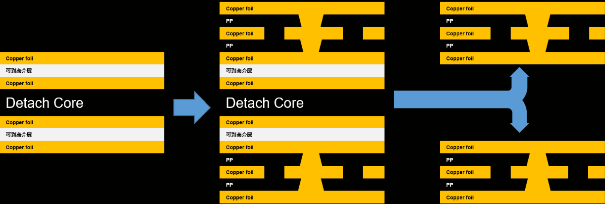
Due to the absence of rigid support, the ultra-thin substrate of coreless boards cannot directly undergo precise circuit patterning and lamination. Therefore, a peelable carrier (Detach Core) must be introduced as temporary support—a defining feature of its manufacturing process.
During production, multilayer circuits are simultaneously built up and patterned on both sides of the carrier to form the target odd-layer structure (e.g., 3 or 5 layers). Finally, the carrier is removed through debonding and singulation steps to obtain a pure coreless ultra-thin HDI board. Compared to core-based boards, coreless boards require additional steps such as carrier lamination, removal, and precision singulation, resulting in a longer process flow and significantly higher demands for process accuracy and warpage control.
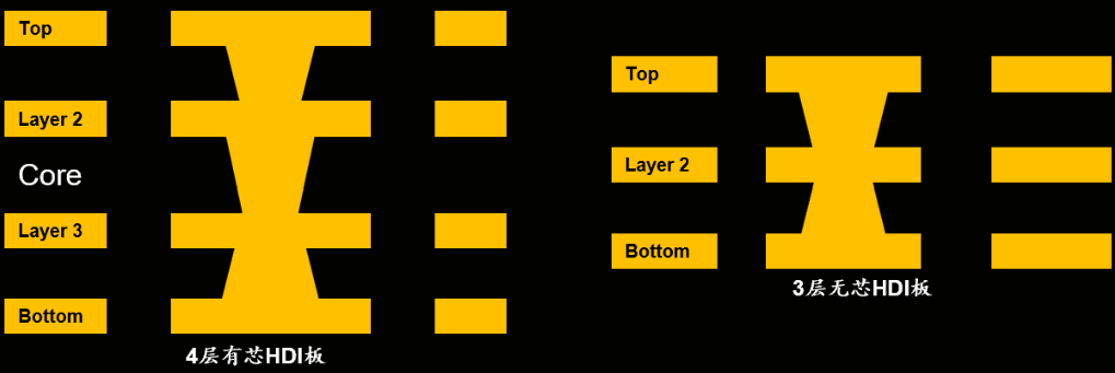
III. Thickness Limits: Divergent Capabilities in Ultra-Thin Design
Constrained by the physical properties of core materials and mainstream equipment capabilities, there is a clear generational gap between the two in terms of thinness.
Currently, the thinnest processable core thickness in the industry is about 40μm, with stable mass production typically ≥50μm. Due to this lower limit, the minimum finished thickness of a standard 4-layer any-layer core-based HDI board is only around 170μm, encountering a natural bottleneck in ultra-thin design.
Coreless boards, however, bypass this limitation entirely by eliminating the core and leveraging peelable carrier technology. For example, a 3-layer coreless HDI board can achieve a finished thickness as low as 115μm, offering exceptional ultra-thin advantages and enabling feasible solutions for extremely lightweight end products.
IV. Advantages and Disadvantages: Rational Trade-offs Between Performance and Cost
1. Core-Based HDI: High Reliability, Low Cost, Mass-Producible
Advantages: The solid core provides strong mechanical strength, excellent resistance to bending, impact, and moisture/heat, along with controllable warpage and outstanding overall reliability—making it suitable for harsh environments. Additionally, its mature processes, universal production lines, high yields, and low marginal costs deliver significant economies of scale.
Limitations: Core thickness constraints prevent extreme thinness, and limited structural flexibility makes it difficult to meet cutting-edge demands for ultra-high density and ultra-thin packaging.
2. Coreless HDI: Extreme Thinness, High-Density Interconnects, Ideal for Advanced Applications
Advantages: The coreless architecture enables extreme thinness. Combined with high-frequency/high-speed materials like ABF and fine-line processes, it achieves smaller line widths/spaces, higher routing density, and lower signal loss, delivering superior high-frequency performance—making it ideal for advanced high-speed digital and RF applications. It also supports odd-layer designs to accommodate specialized circuit topologies.
Limitations: Lacking rigid support, the board is relatively soft and prone to warpage, with yield heavily dependent on warpage control. Additional carrier materials and specialized processes significantly increase production line modifications, material consumption, and labor costs, making it unsuitable for high-volume, general-purpose products.
V. Application Landscape: Clear Division Between Mainstream and High-End Markets
In today’s HDI industry, core-based boards account for over 95% of the market share, serving as the absolute mainstream, while coreless boards remain a niche, high-end complement—with highly differentiated application scenarios.
1. Mainstream Applications of Core-Based HDI
Leveraging high reliability, cost-effectiveness, and stable mass production capabilities, core-based HDI is widely used in cost-sensitive, reliability-critical, and high-volume fields such as smartphone motherboards, automotive electronics, industrial control systems, standard communication modules, and consumer electronics—forming the cornerstone of HDI markets in consumer, industrial, and automotive sectors.
2. Mainstream Applications of Coreless HDI
Capitalizing on ultra-thin profiles, high density, and high-frequency/high-speed characteristics, coreless HDI focuses on advanced chip packaging and high-performance computing/RF modules. Typical applications include AI GPU graphics cards, high-performance HPC server processors, 5G/6G high-frequency base station chips, ASIC mining chips, and high-end memory packaging—all requiring ultra-high precision.
VI. Technological Evolution: Converging Paths with Expanding Boundaries
Core-based and coreless HDI are not in a simple replacement relationship but represent two distinct technological paths developed for different needs—and their boundaries are continuously blurring due to advances in materials, equipment, and processes.
On one hand, core-based HDI continues to push toward thinner designs—using thinner core materials and optimized dielectric stacking to gradually narrow the thickness gap with coreless boards. On the other hand, coreless HDI is improving warpage issues through auxiliary support layers, enhanced lamination stress control, and refined carrier removal techniques, progressively extending into higher layer counts, larger panel sizes, and more demanding reliability applications.
VII. Summary of Key Differences
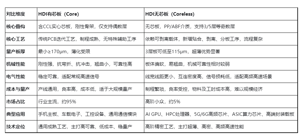
Core-based HDI represents a robust evolution of traditional PCB technology, valued for its high reliability, cost efficiency, and ease of mass production—making it suitable for the vast majority of general-purpose high-density interconnect applications and serving as the backbone of industry supply. Coreless HDI, in contrast, is a cutting-edge solution tailored for ultra-thin, high-density, and high-frequency demands, specializing in advanced chip packaging and high-performance computing/RF niches.
With continuous advancements in substrate technology, precision manufacturing, and process control, both approaches will address their respective limitations and expand their application boundaries, ultimately establishing a long-term complementary landscape where “core-based dominates general applications, while coreless excels in high-end scenarios.”
trending news
Stator-Coreless Axial Flux Motor: PCB Winding Structure, Key Design Considerations, and Application Prospects
Contact Us