



Sorry, no sales person is available right now to take your call. Pls leave a message and we will reply to you via email as soon as possible.
Home/ PCB News/ High-Speed PCB Stackup Design: Core Principles, Standard Layer Arrangements, and Engineering Practice Guide
High-Speed PCB Stackup Design: Core Principles, Standard Layer Arrangements, and Engineering Practice Guide
2026-05-20
Design Principles
PCB fabrication relies on high-temperature and high-pressure lamination processes. Different base materials, copper foils, and prepregs inherently exhibit varying coefficients of thermal expansion (CTE). If the stack-up structure is asymmetric, uneven stress distribution occurs during cooling after high-temperature lamination, leading to board warpage, bending, and localized deformation. Deformed PCBs directly cause misalignment in SMT solder paste printing, component placement errors, cold solder joints, voids, and mounting offsets. In severe cases, entire boards become scrap, drastically reducing mass production yield.
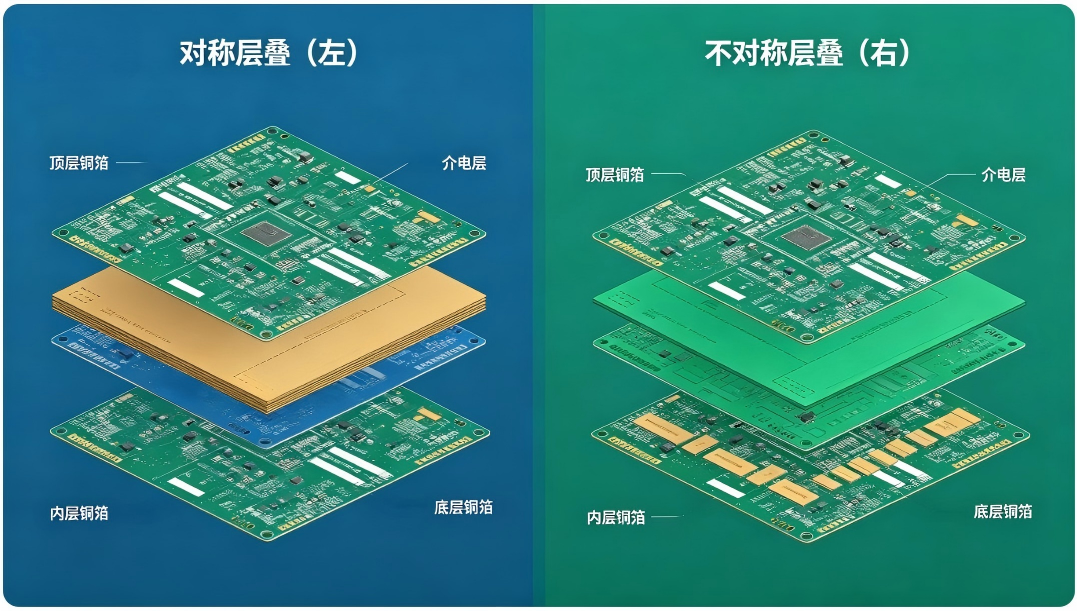
Symmetry Verification Criteria
Using the board’s central axis as a reference, the total copper thickness and total dielectric thickness at symmetrical upper and lower positions must be identical;
The placement positions and layer sequence of core laminates and prepregs must correspond symmetrically above and below;
Dielectric materials, glass weave styles, and nominal thicknesses at symmetrical positions must not differ.
Golden Rule #2: All Signal Layers Must Be Adjacent to a Solid Reference Plane—Direct Adjacency Between Signal Layers Is Prohibited
All high-speed and low-speed signal routing layers must be immediately adjacent to a solid, continuous reference plane (preferably a ground plane, GND) to provide a low-impedance, uninterrupted return path for signals. Additionally, the shielding effect of the plane suppresses interlayer crosstalk and internal/external electromagnetic interference.
It is strictly forbidden to place two signal layers directly adjacent without isolation. Without a reference plane between them, electromagnetic coupling intensifies significantly, severely worsening high-frequency crosstalk and directly compromising high-speed signal timing and integrity, resulting in transmission bit errors and signal jitter.
Special Scenario Compatibility Rules
Only in low-frequency scenarios such as low-speed digital boards or pure power boards, and only under extreme routing resource constraints, may adjacent signal layers be temporarily used—but orthogonal routing (perpendicular crossing between layers) must be strictly enforced to minimize interlayer coupling interference. All high-speed, high-frequency, and differential signal applications strictly prohibit directly adjacent signal layers.
Standard Stack-ups for 3- and 4-Layer Boards (Industry-Standard Mass Production Solutions)
Four-layer boards are the mainstream choice for consumer electronics, industrial control, general industrial equipment, and common hardware projects, offering an optimal balance of structural simplicity, cost control, performance, and manufacturing stability. They represent the most cost-effective solution for medium-to-low-speed circuits. The following industry-standard stack-up is the only universally accepted configuration, with no alternative optimization options.
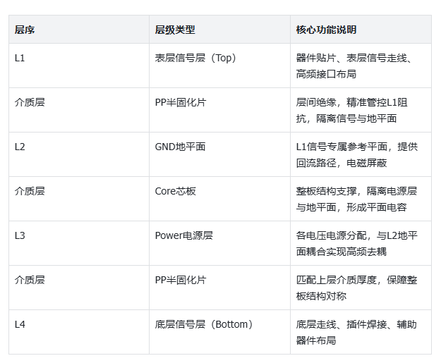
Standard 4-Layer Stack-up Sequence (Top to Bottom)
In-Depth Analysis of Core Structure
The industry-standard Sig-GND-PWR-Sig configuration is the optimal solution for 4-layer boards: L1 top-layer signals use the solid L2 ground plane as their dedicated reference, while L4 bottom-layer signals form stable return paths via the board-wide ground network. Both signal layers achieve precise impedance control and excellent electromagnetic shielding. Additionally, the L2 ground plane and L3 power plane are tightly coupled through the core dielectric, forming a low-parasitic, high-frequency-performance planar capacitor that effectively compensates for the high-frequency limitations of discrete capacitors and suppresses power supply noise.
Planar Capacitance Calculation Formula
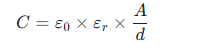
Parameter Definitions: (vacuum permittivity);
 is the dielectric thickness between power and ground planes. For example, with a coupling area of 100mm × 100mm and a core thickness of 0.4mm, the planar capacitance can reach several hundred pF. Without the parasitic inductance of discrete components, its high-frequency decoupling performance far exceeds that of standard surface-mount capacitors, making it a core element for noise suppression in high-speed circuits.
Dielectric Thickness Selection Guidelines (Mass Production Standards)
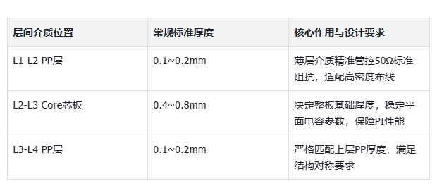
Industry-standard 1.6mm board thickness configuration: 0.2mm prepreg on top and bottom, 0.8mm core in the middle, paired with standard 0.035mm copper foil. This combination fully accommodates manufacturing process tolerances and represents the most versatile standard configuration.
Critical Pitfall to Avoid: Do not use prepreg thicker than 0.4mm. Thick dielectrics increase the distance between signal layers and reference ground, causing 50Ω trace widths to expand to 8–10 mils, severely consuming routing space and failing to meet high-density routing requirements. Standard projects should prioritize thin prepregs of 0.1–0.2mm.
IV. Mainstream 6-Layer Stack-ups (Comparative Selection of Two Configurations)
Six-layer boards offer ample inner-layer routing resources, suitable for multi-rail power, high-density, and medium-to-high-speed signal applications. They are the mainstream choice for industrial control, automotive electronics, and high-speed consumer hardware. The industry primarily adopts two configurations: Balanced General-Purpose and Shielded EMI-Resistant, tailored to different performance requirements.
Option A: Classic Balanced Type (Industry Preferred, Covers 90% of Mass Production Projects)
Stack-up Sequence: L1 Signal → L2 GND Plane → L3 Inner Signal → L4 Power Plane → L5 GND Plane → L6 Signal
Core Advantages
Fully symmetric structure ensures uniform lamination stress, eliminating warpage risk and guaranteeing stable yield;
All signal layers are adjacent to reference planes, ensuring complete return paths and high-precision impedance control;
Dual ground planes effectively absorb magnetic flux lines, suppressing interlayer crosstalk and electromagnetic radiation, delivering balanced SI/PI/EMC performance;
Ample routing resources accommodate both high-density layout and high-speed signal transmission needs.
Applicable Scenarios
Ideal for most medium-to-high-speed circuits, industrial equipment, consumer electronics, and general industrial control projects. It is the standardized optimal solution balancing performance, cost, and manufacturability.
Option B: Multi-Ground Shielded Type (Dedicated for Stringent EMC Environments)
Stack-up Sequence: L1 Signal → L2 GND Plane → L3 Inner Signal → L4 GND Plane → L5 Power Plane → L6 Signal
Core Advantages
Dual-ground shielding structure provides more complete signal return paths and exceptional interlayer electromagnetic isolation, significantly suppressing high-frequency radiation, spatial interference, and crosstalk. Outstanding EMC immunity makes it suitable for complex electromagnetic environments.
Key Limitations
Only three effective signal routing layers (L1, L3, L6), limiting routing capacity for high-density designs;
Higher difficulty in achieving symmetric dielectric structure, requiring precise lamination parameter calibration and stricter process compatibility;
Single concentrated power plane complicates multi-rail power segmentation, offering only average power integrity performance.
Applicable Scenarios
Dedicated to stringent EMC environments, automotive high/low-voltage hybrid circuits, industrial equipment in strong interference settings, and low-density projects where EMI resistance is the primary requirement.
V. Core Design Principles for 8+ Layer High-End PCB Stack-ups
The design of 8+ layer high-count PCBs consistently adheres to two fundamental rules: structural symmetry and alternating signal-plane arrangement. By adding ground planes, power planes, and inner signal layers, these boards support ultra-high-density, ultra-high-speed, and multi-rail power applications (e.g., servers, high-speed communications, AI hardware).
Industry-Recommended 8-Layer Stack-up
L1 Top Signal → L2 GND Plane → L3 Inner Signal → L4 Power Plane → L5 GND Plane → L6 Inner Signal → L7 Power Plane → L8 Bottom Signal
This strictly follows the Sig-GND-Sig-PWR-GND-Sig-PWR-Sig alternating principle—no signal layers are directly adjacent, and every signal layer has an adjacent reference plane, structurally eliminating interlayer crosstalk and ensuring high-speed signal integrity.
Core Guidelines for Advanced High-Speed Design
All high-frequency, high-speed, differential, and clock signals should be routed as stripline structures sandwiched between two ground planes. Routing between power and ground planes is strictly prohibited. Dual-ground shielding minimizes return loop area, parasitic inductance, and provides optimal EMI shielding—the standard configuration for ultra-high-speed signals.
Universal Golden Rules for All Layer Counts
Symmetry Baseline: Full symmetry about the board’s central axis to prevent lamination warpage and manufacturing defects;
Alternating Arrangement: Signal layers and reference planes alternate—no direct adjacency between signal layers;
More Grounds, Fewer Power Planes: Prioritize more ground planes than power planes to ensure return paths and shielding;
High-Speed Near Ground: Route high-speed signals adjacent to ground planes—never use power planes as reference;
Tight Plane Coupling: Place power and ground planes as close as possible to maximize planar capacitance and optimize high-frequency PI performance.
VI. Ground Planes and Signal Return Paths: The Physical Foundation of High-Speed Circuits
Many engineers simplistically define ground planes as "0V reference," which is incomplete. In high-speed circuits, the core function of a ground plane is to provide a low-impedance, continuous, minimal-loop return path for high-frequency signals. Over 90% of high-speed EMC failures, signal jitter, and crosstalk issues stem from incomplete return paths.
Signal transmission forms a closed loop: after the driver sends current through the trace to the receiver, the return current must flow back to the driver to complete the circuit. In high-speed scenarios, return paths do not follow the lowest-resistance rule but instead adhere to high-frequency physical principles.
Key Characteristics of High-Frequency Return Paths
Low-frequency signals (DC–kHz) follow the lowest-resistance path; high-frequency signals (MHz+) are constrained by skin effect and minimum inductance principles, so return currents concentrate strictly in the ground plane region directly beneath the signal trace, forming the smallest possible current loop to minimize parasitic inductance and electromagnetic radiation.
Typical Engineering Issue: EMC Failure Due to Ground Plane Splitting
Radiation超标, signal distortion, and other issues in high-speed interfaces (USB, HDMI, DP, clocks, differential buses) often originate from high-speed signal return paths crossing ground plane splits. When the ground plane contains slots, splits, or large voids, high-frequency return currents cannot follow the shortest path directly underneath and must detour around the split, creating an oversized current loop. This loop acts as an antenna, radiating electromagnetic waves and directly causing EMC radiation test failures and increased signal jitter.
Mandatory Design Rule: The ground plane directly beneath all high-speed differential signals, high-frequency clocks, and high-speed buses must be continuous, unsplit, slot-free, and free of large voids. If analog, digital, and power grounds must be separated, high-speed signals must never cross ground splits—this is the fundamental rule for avoiding high-speed EMC issues.
VII. High-Speed Transmission Line Structures and Impedance Matching Principles
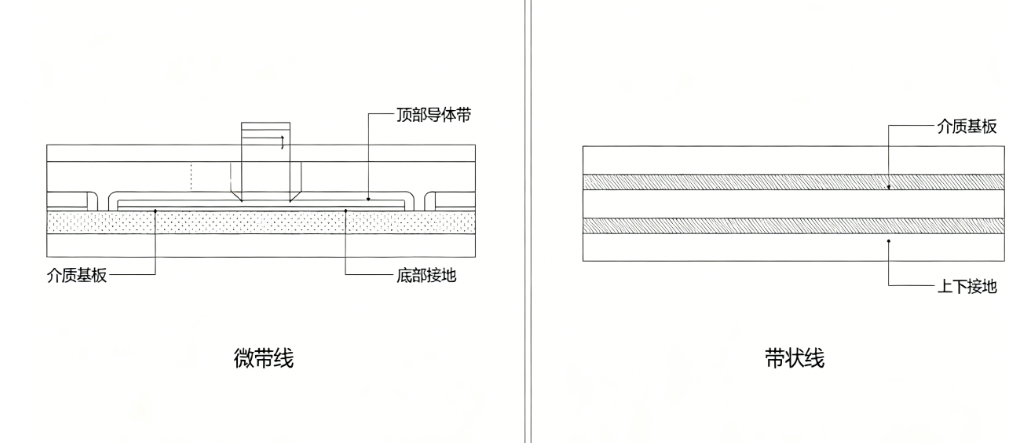
Once the stack-up is finalized, precise impedance matching must be performed based on material parameters. PCB high-speed transmission lines fall into two categories: microstrip and stripline, which differ significantly in structure, electrical characteristics, and application—forming the foundation of high-speed routing.
1. Microstrip (Surface Transmission Structure)
Definition: A trace on the PCB surface (L1/L4), with air on one side and an inner solid ground plane as the sole reference below.
Core Characteristics
Electric field distributed between air and FR-4 dielectric, resulting in lower effective dielectric constant, shorter signal delay, and faster speed;
No upper dielectric shielding—more susceptible to external interference and higher self-radiation;
Visible surface traces facilitate debugging, modification, and testing—making it the mainstream choice for surface high-speed signals.
2. Stripline (Inner-Layer Transmission Structure)
Definition: An inner-layer trace fully enclosed between two ground planes and dielectric material, isolated by surrounding dielectric and ground planes.
Core Characteristics
Trace fully embedded in FR-4 dielectric—electric field contained internally, providing inherent excellent EMI shielding and superior EMC performance;
Stable impedance unaffected by external environment or routing interference, with excellent interlayer crosstalk suppression;
Slightly slower signal speed than microstrip—optimal for high-frequency, ultra-high-speed, and precision signals.
3. Impedance Parameter Variation Trends
Microstrip and stripline share consistent impedance trends. The impact of key parameters on impedance is as follows:
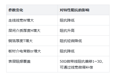
Hard Requirement for Engineering Practice: Never manually calculate impedance using formulas. Manual calculations ignore critical corrections like copper roughness, dielectric edge effects, solder mask compensation, and process tolerances, leading to large errors. Mass production designs must use professional tools like Si9000, Saturn PCB Toolkit, or KiCad’s built-in impedance calculator with actual fab parameters for accurate results.
VIII. Standardized Stack-up Design Workflow
Based on PCB mass production tolerances, high-speed design rules, and project implementation experience, this section outlines a standardized, actionable, and manufacturable stack-up design workflow to avoid design pitfalls and production risks.
Step 1: Confirm Overall Board Thickness
Determine board thickness based on product mechanical clearance, housing constraints, and thermal requirements. Prefer industry-standard thicknesses: 1.6mm (mainstream), 1.0mm, 0.8mm, or 2.0mm. Avoid non-standard thicknesses to prevent increased process costs and reduced yield.
Step 2: Select PCB Layer Count
Choose layer count based on routing density, number of power rails, signal speed, EMC requirements, and cost budget, following the principle of "sufficient but not excessive" to balance performance and cost.
Step 3: Assign Layer Types
Strictly follow symmetry and signal-plane alternation principles when assigning top/bottom signals, inner signals, ground planes, and power planes. Prioritize sufficient ground planes and ensure high-speed signals are placed near ground.
Step 4: Select Dielectric Materials and Thicknesses
Do not use custom non-standard dielectric thicknesses. All cores and prepregs must be selected from the fab’s official standard catalog (e.g., 106, 1080, 2116 glass styles), strictly matching symmetry and total thickness requirements to ensure stable lamination.
Step 5: Impedance Simulation and Fine-Tuning
Import the fab’s measured Dk (dielectric constant) and Df (loss factor) into professional impedance tools to calculate trace widths. Fine-tune dielectric thickness to keep standard 50Ω traces within the optimal 4–8 mil range, balancing routing density and process compatibility.
Step 6: Fab Stack-up Review (Critical—Do Not Skip)
Submit the preliminary stack-up to the PCB fab’s engineering team for Build-up review to confirm manufacturability, verify lamination tolerances, and correct material parameter deviations—preventing design-manufacturing mismatches.
Step 7: Lock Down Stack-up Parameters
Finalize and lock the confirmed stack-up thicknesses, material types, impedance parameters, and copper specifications in the EDA tool as the sole reference for all routing, simulation, and debugging—no changes allowed during design.
Ultimate Pitfall to Avoid: Never estimate dielectric constant subjectively. Dk values for FR-4 can vary by over 0.2 between fabs and production batches, directly causing impedance failure and signal anomalies. All design parameters must be based on the fab’s official measured reports to ensure design-manufacturing consistency.
IX. Typical High-Speed Stack-up Failure Cases: Root Causes and Mass Production Remediation
Based on high-speed project mass production debugging, EMC pre-compliance testing, SI simulation validation, and factory rework experience, this section summarizes eight common stack-up design failure scenarios. Each follows a standardized template—「Failure Phenomenon – Root Cause – Remediation – Prevention」—to precisely identify design flaws, define actionable fixes, and establish preventive measures, resolving most performance and yield issues caused by stack-up defects. This approach aligns with engineering troubleshooting, post-mortem analysis, and standardized design practices.
Case 1: Asymmetric Layers Cause Board Warpage, Leading to SMT Voiding and Cold Joints
Failure Phenomenon: PCB warpage exceeds 0.8% after reflow, causing solder paste misalignment and BGA placement errors in SMT. Batch defects include voids, cold joints, and bridging, drastically reducing yield. Low-speed boards show no obvious issues, but high-speed boards fail frequently.
Root Cause: Stack-up violates central-axis symmetry—copper thickness, prepreg/core thickness, and copper coverage differ significantly between top and bottom. Some designs concentrate large copper areas on one side without balancing copper on the opposite layer, exacerbating thermal stress.
Remediation: 1. Redesign stack-up to ensure mirror symmetry in copper thickness, dielectric thickness, and material type across the central axis; 2. Add balancing copper on the symmetric layer opposite large copper pours to counteract thermal expansion stress; 3. Work with the fab to optimize lamination profile, controlling cooling rate to ≤1°C/min to release residual stress.
Prevention Rule: Mandate symmetry verification after stack-up finalization—copper thickness, dielectric thickness, and material specs must match exactly. High-density large copper pours must include balancing copper; single-sided copper imbalance is prohibited.
Case 2: Adjacent Signal Layers Cause Excessive Crosstalk and Bit Errors
Failure Phenomenon: DDR, PCIe, and high-speed differential buses malfunction—high bit error rates, collapsed eye diagrams, and excessive jitter. Testing shows interlayer crosstalk as high as -15dB. High-speed links fail to achieve rated speeds, though low-speed functions work normally.
Root Cause: To save layers or increase routing space, the reference isolation plane was omitted, placing two high-speed signal layers directly adjacent without ground shielding. This dramatically increases electromagnetic coupling and severe high-frequency interference.
Remediation: 1. Modify stack-up to insert a solid ground plane between the two signal layers, strictly following signal-plane alternation; 2. If layer count is fixed, enforce strict orthogonal routing on adjacent signal layers—no long parallel runs; 3. Shorten parallel lengths of high-speed traces and add shielding ground vias along critical signals to reduce coupling.
Prevention Rule: Never place signal layers directly adjacent in high-speed/high-frequency designs. Only pure low-speed circuits may temporarily allow adjacency, but must enforce both orthogonal routing and minimized parallel length.
Case 3: High-Speed Signals Cross Ground Splits, Causing EMC Radiation Failure
Failure Phenomenon: USB, HDMI, and high-speed clock interfaces fail radiated emissions tests. Full-system EMC pre-compliance fails. Low-speed signals are unaffected, but radiation worsens under high-temperature conditions.
Root Cause: Poor separation of analog, digital, and power grounds causes high-speed differential and clock traces to cross ground splits. High-frequency return paths are forced to detour, greatly increasing loop area and forming an effective radiating antenna that continuously emits electromagnetic noise.
Remediation:
1. Ensure ground plane under high-speed signals is fully continuous—eliminate splits along signal paths;
2. If ground splits are necessary, reroute high-speed traces to avoid crossing splits;
3. Add high-frequency bridging capacitors across split gaps to restore return paths.
Prevention Rule: Prohibit ground splits, slots, or large voids under all high-speed, differential, and clock signals. Ground splits may only be placed under low-speed traces or unused areas.
Case 4: Excessive Power-Ground Dielectric Thickness Causes High-Frequency PI Noise and Ripple
Failure Phenomenon: Excessive high-frequency power ripple, poor dynamic load response, and occasional high-speed IC resets or crashes. Adding multiple high-frequency decoupling capacitors yields minimal improvement.
Root Cause: Excessive core thickness (>0.8mm) between power and ground planes drastically reduces planar capacitance and increases high-frequency parasitic inductance. This nullifies the high-frequency decoupling capability of the power-ground plane pair, failing to compensate for the high-frequency limitations of discrete capacitors and degrading power integrity.
Remediation:
1. Optimize stack-up to reduce power-ground dielectric thickness, bringing planes closer to increase planar capacitance;
2. Group multi-rail power regions locally to avoid extensive segmentation of a single power plane;
3. Add dense arrays of high-frequency 0402/0201 decoupling capacitors on critical power rails to enhance high-frequency filtering.
Prevention Rule: For high-speed designs, prioritize thin core laminates (0.4–0.6mm) between power and ground to maximize planar capacitance and ensure effective high-frequency noise suppression.
Case 5: Mismatched Dielectric Thickness Causes Impedance Shift and TDR Failure
Failure Phenomenon: Poor impedance consistency across the board—some traces too high/low. TDR tests show excessive variation. Severe signal reflections and timing skew occur, and batch impedance yield is unstable.
Root Cause: Stack-up design used theoretical Dk values and non-standard prepreg/core thicknesses without fab-measured parameters. Thick prepregs also caused uncontrolled spacing between signal and reference planes. Combined with unaccounted copper roughness and missing solder mask compensation, this led to significant impedance deviation.
Remediation:
1. Obtain fab’s batch-specific measured Dk/Df values and recalibrate trace widths and dielectric thickness using Si9000;
2. Replace non-standard thick prepregs with standard 0.1–0.2mm thin prepregs to unify interlayer spacing;
3. Add solder mask and copper roughness compensation to correct impedance偏差.
Prevention Rule: Never use generic theoretical parameters for impedance calculation—always use fab-measured data. All dielectric thicknesses must come from the fab’s standard catalog; custom non-standard stack-ups are prohibited.
Case 6: Inner High-Speed Signals Sandwiched Between Power and Ground Suffer Dual Crosstalk and Radiation Failures
Failure Phenomenon: Inner high-speed differential signals exhibit poor noise immunity, easily coupling with power supply noise. Transmission jitter is high, and both radiated emissions and immunity tests fail.
Root Cause: High-speed traces were placed between power and ground planes without dual-ground shielding. Low- and high-frequency noise from the power plane easily couples into signals, and poor shielding causes significant signal leakage—violating high-speed stripline design rules.
Remediation:
1. Redesign stack-up and routing to implement dual-ground stripline structures for all critical high-speed signals;
2. If layer count is fixed, replace local power plane areas under these signals with ground to provide near-reference;
3. Segment power plane into isolated regions to limit noise propagation.
Prevention Rule: DDR, PCIe, high-speed differential, and clock signals must use dual-ground stripline structures. Never use a power plane as the sole reference.
Case 7: Poor Lamination Structure Causes Delamination and Poor Thermal Reliability
Failure Phenomenon: After reflow or high-temperature aging, PCBs exhibit blistering, delamination, or layer separation. Electrical continuity fails, and failures worsen in high-humidity environments.
Root Cause: Unreasonable mix of thick and thin dielectrics and insufficient resin content in prepregs lead to inadequate resin flow during lamination, causing local resin starvation and voids. Combined with moisture absorption and inadequate oxide treatment, thermal stress triggers interlayer separation.
Remediation:
1. Optimize prepreg-core combinations—use high-resin-content prepregs and avoid extreme combinations like thick cores with thin prepregs;
2. Fab optimizes lamination temperature, pressure, and dwell time to eliminate voids;
3. Add PCB pre-bake step before production (120°C for 2–4 hours) to remove moisture.
Prevention Rule: For high-layer-count or thick boards, avoid extreme thick-thin dielectric combinations. Stack-up review must include resin fill capability assessment to proactively prevent delamination.
Case 8: Insufficient Ground Planes Cause Poor Noise Immunity and High Noise Floor
Failure Phenomenon: High static current fluctuations, elevated signal noise floor, and system resets or communication drops triggered by minor external interference. No hard EMC failure, but overall system stability is poor.
Root Cause: Stack-up design unnecessarily minimized layer count and ground planes, resulting in too many power planes and too few ground planes. Sparse return paths and inadequate shielding lead to high overall ground impedance, preventing effective noise dissipation.
Remediation:
1. Redesign stack-up to add ground planes, implementing the "more grounds, fewer power planes" golden rule;
2. Flood unused inner layers with ground to supplement return paths;
3. Add grounding vias near critical power and signal areas to reduce ground impedance.
Prevention Rule: Prioritize ground plane redundancy in high-speed designs. Consolidate power rails into shared regions rather than dedicating separate power layers, ensuring sufficient ground planes for shielding and return performance.
All high-speed stack-up failures ultimately trace back to five structural flaws: asymmetry, lack of near-ground reference for signals, incomplete return paths, mismatched dielectric ratios, and incorrect material parameter usage. Stack-up design is the root of high-speed PCB performance—routing, simulation, and debugging are merely secondary optimizations. Mass production projects must strictly adhere to symmetry, alternating arrangement, near-ground shielding, and tight plane coupling to proactively prevent failures and structurally guarantee SI/PI/EMC performance and manufacturing stability.
trending news
Contact Us