



Sorry, no sales person is available right now to take your call. Pls leave a message and we will reply to you via email as soon as possible.
Home/ PCB News/ Precision in Every Inch, Excellence through Craftsmanship | BaiNeng YunBoard 12-Layer 3-Stage HDI PCB Empowers Industrial Intelligence Advancement
Precision in Every Inch, Excellence through Craftsmanship | BaiNeng YunBoard 12-Layer 3-Stage HDI PCB Empowers Industrial Intelligence Advancement
2026-05-18
In high-end fields such as industrial automation control, edge computing, precision testing, and industrial communication, equipment demands extremely stringent requirements for stability, integration density, and high-speed transmission performance. As the core interconnect platform of industrial intelligent devices, PCBs serve as the foundation for stable system operation and directly determine the performance ceiling and service life of end products. Addressing industry-critical needs for miniaturization, high computing power, high load capacity, and long-term stable operation of industrial equipment, BaiNeng Cloud PCB proudly launches its 12-layer three-stage HDI board. Combining cutting-edge precision manufacturing processes with rigorous industrial-grade quality control, this solution delivers high-density, high-speed, and highly reliable interconnectivity—breaking through the performance limitations of traditional PCBs and empowering the iterative advancement of high-end industrial intelligent devices.
Precision Process Innovation: Building a Robust Foundation for High-Density Interconnects
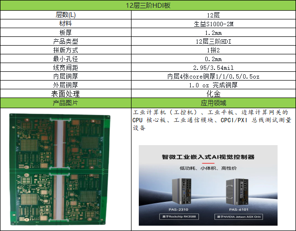
BaiNeng Cloud PCB’s 12-layer three-stage HDI board adopts mainstream advanced sequential lamination technology, integrating precise blind/buried via and microvia technologies to completely overcome traditional PCB limitations in routing space and layer count. Within an ultra-thin 1.2mm profile, it achieves orderly 12-layer circuit stacking and efficient interconnection, effectively eliminating stub-induced interference in high-speed signal transmission. This creates low-loss, low-crosstalk, and highly consistent high-frequency transmission channels—perfectly meeting the demanding requirements of high-end industrial equipment for high-speed, real-time data interaction.
Micron-Level Precision Routing for High-Density, Fine-Pitch Packaging
The product achieves industry-leading hair-thin line fabrication accuracy, with a minimum hole diameter of 0.2mm and tightly controlled line width/space down to 2.95/3.54 mil. It fully supports high-density, fine-pitch component packages such as BGA, QFN, and μBGA. Its meticulously organized multi-layer layout efficiently addresses the challenges of high integration and miniaturization in industrial equipment design, providing solid process support for lightweight, integrated end products.
Gradient Copper Thickness Structure: Balancing Signal Integrity and Power Delivery
The inner layers feature a differentiated gradient copper thickness design of 1/1/0.5/0.5 oz, while the outer layers maintain a stable finished copper thickness of 1.0 oz. This scientifically optimized copper distribution balances high-speed signal integrity with high-current power delivery—ensuring low-loss, high-purity high-frequency signal transmission while significantly enhancing current-carrying capacity in power and ground planes. It also improves overall thermal management, comprehensively supporting long-term, high-load, uninterrupted stable operation.
Rigorous Material Selection: Forging an Industrial-Grade Reliability Shield
Industrial environments constantly expose equipment to harsh conditions such as thermal cycling, high humidity, dust accumulation, and frequent vibration. Material and process stability are therefore critical to ensuring long-term reliability. Adhering strictly to industrial-grade quality standards, BaiNeng Cloud PCB rigorously controls every step—from base material selection to surface finishing—to comprehensively enhance board environmental adaptability and build a robust reliability barrier for end devices.
Base Material Selection: The board uses Shengyi S1000-2M industrial-grade high-performance laminate, featuring an ultra-high Tg of 170°C and an extremely low coefficient of thermal expansion (CTE). This effectively resists board warpage, delamination, and cracking caused by extreme temperature variations. It offers excellent via reliability and outstanding resistance to Conductive Anodic Filament (CAF) formation, with superior moisture/heat resistance, aging resistance, and corrosion resistance—far exceeding standard materials. Additionally, it employs lead-free FR-4 eco-friendly material compliant with green manufacturing standards, offering excellent machinability to ensure high yield and consistent quality in mass production.
Surface Finish: A precision ENIG (Electroless Nickel Immersion Gold) process forms a uniform, dense nickel-gold protective layer. On one hand, it significantly improves surface planarity, eliminating the "dog bone effect" common in traditional HASL finishes, thereby providing a flat, reliable soldering base for fine-pitch components and effectively reducing risks of cold solder joints, voids, or de-wetting. On the other hand, the chemically stable gold layer imparts excellent anti-oxidation, corrosion resistance, and anti-sulfidation properties to solder pads—greatly extending board shelf life and overall equipment lifespan, while ensuring consistent solderability and stable connections throughout years of industrial operation.
Empowering Full-Scale Industrial Applications: Deep Focus on High-End Intelligent Equipment
Leveraging its advantages in high-density design, exceptional stability, and broad scenario adaptability, QJ/BaiNeng Cloud PCB’s 12-layer three-stage HDI board has already achieved large-scale deployment across multiple high-end industrial applications. With proven reliability, it provides core hardware support for performance and quality upgrades of diverse industrial intelligent terminals.
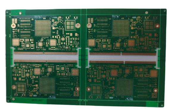
12-Layer 3-Stage HDI Board Product Showcase
Case 1: Core Application in Embedded AI Vision Controllers
In industrial PAS-2310/6101 series embedded AI vision controller projects, this HDI board serves as the central signal interconnect backbone. Its 12-layer high-density routing architecture perfectly accommodates high-end AI computing platforms such as Rockchip RK3588 and NVIDIA Jetson AGX Orin, stably handling multi-channel high-speed signal transmission to enable low-latency, highly synchronized data exchange between computing units and peripheral interfaces. Thanks to its ultra-thin profile and high integration, the board enables compact, low-power, and cost-effective device designs, delivering long-term stable performance in industrial machine vision inspection, intelligent quality control, and automated sorting—achieving bit error rates better than industry standards.
Case 2: CPU Carrier Board Solution for Multi-Core Industrial PCs
Addressing key technical challenges in high-end multi-core industrial PCs—including high-density routing, high-current delivery, and continuous thermal management—this 12-layer three-stage HDI board offers a comprehensive solution. Its three-stage sequential lamination enables efficient interconnection between CPU cores and high-speed interfaces like DDR and PCIe, while micron-level routing precision fully matches fine-pitch BGA packaging requirements. The gradient copper structure optimizes power and ground plane layouts, effectively suppressing crosstalk and enhancing both current-carrying capacity and heat dissipation—ensuring 24/7 high-load operation in industrial environments with exceptional adaptability and stability.
Case 3: Backplane Application in CPCI/PXI Bus-Based Precision Test Equipment
In high-end CPCI/PXI bus test and measurement systems, this board provides critical interconnect reliability for the backplane. The ENIG finish ensures excellent solder joint stability and wear resistance, reliably withstanding frequent module insertion/removal and high-vibration conditions without connector loosening or failure. Combined with the high-Tg base material’s superior thermal stability, it maintains precise and consistent bus signal integrity despite prolonged operational temperature fluctuations—fully meeting the industry’s strict standards for data accuracy, repeatability, and stability in test equipment.
Beyond these core applications, this HDI board is also widely compatible with industrial tablets, edge computing gateways, industrial communication modules, and intelligent measurement & control devices—comprehensively enabling the next generation of industrial intelligent equipment to achieve miniaturization, high integration, superior performance, and enhanced reliability.
Precision Manufacturing, Worry-Free Delivery: Empowering the Future of Industrial Intelligence Together
With years of deep expertise in high-end precision PCB R&D and manufacturing, BaiNeng Cloud PCB steadfastly upholds the philosophy of “micron-level precision, industrial-grade standards.” We offer end-to-end customized services—from design optimization and process adaptation to precision prototyping and volume production—ensuring uncompromised quality and on-time delivery.
QJ/BaiNeng Cloud PCB’s 12-layer three-stage HDI board represents the deep integration of advanced manufacturing processes, premium materials, and real-world industrial demands—a testament to our technical expertise and commitment in the high-end industrial PCB domain. We meticulously craft every board to fortify the performance and reliability foundation of industrial intelligent devices, helping customers enhance their core product competitiveness and jointly shaping the future of industrial intelligence.
trending news
Contact Us