



Sorry, no sales person is available right now to take your call. Pls leave a message and we will reply to you via email as soon as possible.
Home/ PCB News/ High Power Consumption of AI Drives Material Innovation: Ceramic Substrates Usher in a New Cycle of PCB Replacement and Domestic Substitution
High Power Consumption of AI Drives Material Innovation: Ceramic Substrates Usher in a New Cycle of PCB Replacement and Domestic Substitution
2026-05-15
The core competition in AI hardware has long centered on GPU computing power, HBM memory, advanced packaging, and optical interconnects. However, as AI chip power consumption continues to rise, bottlenecks in underlying materials are becoming increasingly evident: traditional epoxy resin PCBs can no longer handle the combined thermal, electrical, and signal stresses of AI hardware operating at 3000W-level ultra-high power. Upgrading base materials has thus become an essential requirement for industry iteration.
According to NVIDIA’s product roadmap, the next-generation Rubin GPU will reach a power consumption of 2850W, with the Rubin Ultra variant exceeding 3000W—far surpassing the typical 2000W household induction cooktop—and overall power demands are expected to keep rising. The high-density thermal load generated by such extreme computing performance has completely breached the performance limits of conventional electronic materials. This pressure propagates layer by layer from the chip down through package substrates, PCBs, connectors, and power delivery systems, compelling a comprehensive upgrade of the entire underlying material ecosystem.
All market assessments in this article represent an analytical framework for industry observation only and do not constitute any investment advice.
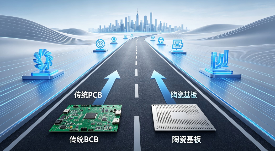
I. Traditional PCB Performance Has Peaked; Ceramic Hybrid Lamination Emerges as the Optimal Solution
Traditional PCBs have long served as the foundational substrate in the electronics industry due to their mature manufacturing processes and cost-effectiveness. However, under the extreme conditions of ultra-high power consumption, high frequency, and high speed demanded by AI applications, their inherent limitations are fully exposed: susceptibility to softening and warping at high temperatures, high dielectric loss during high-frequency transmission, and insufficient signal stability. As single-GPU power consumption enters the 2500W–3000W range, PCBs simultaneously endure triple extreme loads—thermal stress, high current, and high-frequency signals—pushing material performance to its physical limits.
Ceramic substrates are not a new material. Their high-temperature resistance, high thermal conductivity, low dielectric loss, and strong structural stability make them highly suitable for the extreme operating conditions of AI servers. However, due to relatively high costs, complex processing techniques, and limited scalability, the industry has not adopted full ceramic substrate replacement of PCBs. Instead, it has widely embraced a gradual, pragmatic approach: hybrid lamination of HDI PCBs with ceramic substrates. In high-heat-flux and high-current critical zones, ceramic substrates enhance performance, while conventional routing areas retain the cost advantages of PCBs—achieving an optimal balance among performance, reliability, and economics.
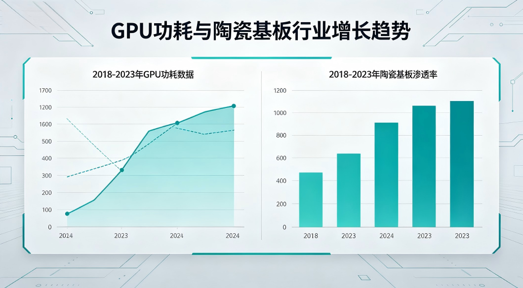
In current AI server boards, the substitution ratio of ceramic substrates for traditional PCBs has already approached 30% and will continue to expand as chip power consumption increases. Breaking down the value drivers, 60% stems from thermal management optimization and 40% from signal integrity enhancement. The adoption pace of this technology is tightly coupled with GPU power curves, representing a classic case of necessity-driven substitution rather than conceptual upgrading.
China’s ceramic substrate industry is rapidly closing the gap in high-end processes and mass production capabilities. Leading domestic manufacturers have already achieved key technological breakthroughs and commercial implementation. As a representative enterprise with full-chain support capabilities, Baineng Yunban has established a mass production system for ceramic substrates tailored to high-power AI scenarios, comprehensively covering the four mainstream technologies: HTCC, LTCC, DBC, and AMB. It can stably produce 1–6 layer high-precision ceramic PCBs using advanced thermally conductive base materials such as alumina, aluminum nitride, and silicon nitride. The company possesses core competencies including integrated ceramic-PCB hybrid lamination processes, precision circuit fabrication, and high-reliability surface treatment—effectively addressing critical pain points in AI hardware such as high-temperature warpage, insufficient heat dissipation efficiency, and high-frequency signal distortion. Its products meet the stringent performance and delivery standards required for AI server boards, power modules, and advanced packaging.
II. Two Core Application Scenarios: GPU Bottom and Orthogonal Backplane Drive Large-Scale Adoption
Current industrial adoption of ceramic substrates prioritizes two high-load scenarios in AI servers. Through localized hybrid lamination strategies, system reliability is significantly enhanced at controllable costs, offering a clear industrial logic and high implementation certainty.
1. High-Heat Core Area Beneath the GPU
The area beneath the GPU is the focal point of heat and current concentration in the entire server, imposing extremely high demands on thermal stability, flatness, and thermal conductivity of the substrate. It is also where traditional PCB failures occur most frequently. Although ceramic substrates cost 18–20 times more than high-end HDI PCBs, targeted localized replacement increases the total board cost by only 30%–35%, making large-scale deployment economically viable.
To address the extreme operating conditions of ultra-high heat flux and ultra-high current beneath GPUs, leading domestic manufacturers have already iterated customized solutions. Baineng Yunban’s high-thermal-conductivity ceramic substrate solutions based on aluminum nitride and silicon nitride leverage high-precision etching, thin-profile processing, and highly stable metallization processes to effectively reduce system thermal resistance and suppress high-temperature deformation—ensuring structural stability and high-frequency signal purity under ultra-high-power operation, precisely meeting the localized load-bearing and thermal requirements of NVIDIA’s high-power Rubin-series GPUs.
2. Orthogonal Backplane Area in Servers
Orthogonal backplanes primarily address system-level power delivery and high-frequency signal transmission bottlenecks in AI servers. The industry typically replaces 2–3 power and ground layers with ceramic substrates. While material costs are 8–10 times higher than standard PCBs, hybrid integration raises the total board value by only 20%–25%. As AI systems evolve toward rack-scale cluster deployments, system power stability and low-loss transmission capability are gradually overtaking single-chip computing power as the primary constraints on overall system performance.
Orthogonal backplanes impose stringent requirements on dielectric properties, insulation performance, and loss characteristics of base materials. Dedicated ceramic substrates designed for high-load cluster servers offer low dielectric constant, low loss, and high insulation—effectively reducing power delivery losses and suppressing high-frequency crosstalk, making them suitable for continuous, high-load operation in AI rack-scale systems. Moreover, these products seamlessly integrate with mainstream PCB hybrid lamination processes and server board design frameworks, demonstrating outstanding scenario compatibility and engineering feasibility.
III. CoWoP Advanced Packaging: Ceramic Core Layers Unlock High-Value Substitution Opportunities
Compared to partial substitution in server boards, CoWoP (Chip-on-Wafer-on-Substrate) advanced packaging represents the highest-value and most technologically demanding direction in the ceramic substrate market. Traditional pure ABF substrates suffer from warpage, resin bleeding anomalies, and declining yield in high-stack, high-density packaging architectures, rendering them inadequate for next-generation ultra-high-power AI chip packaging requirements.
The industry’s mainstream technical evolution path involves a hybrid structure combining an HTCC ceramic core layer with ABF outer layers: multi-layer ceramic substrates serve as the structural backbone to ensure dimensional accuracy and thermal stability, while ABF layers enable high-density, fine-pitch routing—balancing structural reliability with routing flexibility. In this architecture, ceramic substrates account for 65%–70% of the total substrate value, and overall procurement costs are 70%–80% higher than pure ABF solutions, making them a mandatory prerequisite for next-generation advanced packaging upgrades.
Compared to glass substrates, which face longer industrialization cycles, ceramic substrates offer faster implementation timelines and stronger supply chain adoption certainty. They have already entered NVIDIA’s mainstream product supply chain. To tackle the “bottleneck” challenges in CoWoP packaging, leading domestic manufacturers have proactively invested in R&D. Notably, Baineng Yunban has successfully overcome core HTCC multi-layer co-firing technologies, solving industry pain points such as high-precision interlayer alignment, precise matching of coefficients of thermal expansion (CTE), and process synergy with ABF hybrid lamination. The company now provides high-flatness, low-warp, high-reliability ceramic core layer samples and small-batch production services, supporting product iteration and validation for high-end advanced packaging customers and helping break the long-standing technological monopoly held by overseas suppliers.
IV. Competitive Landscape: Kyocera’s Monopoly and China’s Three-Tier Breakthrough Strategy
The high-end AI ceramic substrate market is currently highly concentrated, with HTCC ceramic core layers for CoWoP packaging being almost exclusively mass-produced by Japan’s Kyocera. Domestic manufacturers have long been constrained by comprehensive barriers—including multi-layer co-firing processes, precision machining accuracy, long-term reliability, and high-end customer certifications—and have yet to establish mature mass production capabilities comparable to international peers.
China’s import substitution journey can be divided into three tiers, with technical difficulty decreasing from top to bottom and market feasibility increasing accordingly:
Tier 1: CoWoP Ceramic Core Layers
This is the highest-end segment, featuring extremely high technical and certification barriers and representing Kyocera’s core monopoly domain. Key evaluation criteria include HTCC stack layer count, dimensional accuracy, mass production yield, long-term reliability, and validation progress with leading packaging customers—making it the primary focus of long-term domestic R&D efforts.
Tier 2: AI Server Hybrid Ceramic Substrates
This segment features moderate process barriers and shorter validation cycles, serving as the key entry point for domestic players into high-end AI supply chains. Core competitive dimensions include ceramic sintering precision, fine machining capabilities, PCB hybrid compatibility, and long-term reliability certification. Currently, domestic leaders like Baineng Yunban have completed multiple iterations of AI board ceramic substrate solutions. With full-process coverage, customized R&D, rapid sample validation, and scalable mass production capabilities, they have become the main force driving domestic substitution in this segment, offering strong rapid-deployment advantages.
Tier 3: Upstream Supporting Materials and Equipment
Upstream segments—including ceramic powders, specialized slurries, metallization processes, precision sintering equipment, and performance testing—offer strong demand certainty and lower entry barriers, making them the first areas where China’s industrial chain has achieved breakthroughs and continues to benefit.
V. Key Tracking Metrics: Capturing the Pace of Industrial Evolution
The necessity of ceramic substrates in AI applications is now firmly established. Future focus should shift from debating market growth potential to tracking five core indicators to accurately gauge industrial evolution:
1. Continuous increase in ceramic substrate adoption rates across three key scenarios—GPU bottom, orthogonal backplane, and package substrates—as NVIDIA rolls out new-generation platforms;
2. Technical and mass production breakthroughs by second- and third-tier suppliers beyond Kyocera, gradually loosening the oligopolistic market structure;
3. Accelerating progress in domestic vendors’ sample testing, pilot production, and customer integration, marking the transition of import substitution into tangible implementation;
4. Leading server board, PCB, and advanced packaging manufacturers accelerating ceramic hybrid technology collaborations to drive large-scale solution adoption;
5. Continuous cost reduction in ceramic substrate production, enabling PCB substitution ratios to exceed 30% and steadily rise further.
VI. Industry Summary: Ultra-High Power Redefines Base Material Value; Domestic Substitution Reaches an Inflection Point
Historically, value creation in AI hardware has been concentrated in visible core segments like GPUs, HBM, and optical modules. In the new era of 3000W-class ultra-high power, however, thermal management efficiency, power delivery stability, and high-frequency signal integrity have become the primary bottlenecks limiting system performance—triggering a comprehensive revaluation of long-overlooked base materials.
This industrial evolution follows a clear and closed-loop logic: continuous AI chip performance scaling → sharply rising chip power and thermal density → performance limits and failure of traditional PCB materials → localized large-scale substitution by ceramic substrates → a definitive window of opportunity for domestic high-end electronic materials.
During this critical transformation window, domestic manufacturers possessing integrated capabilities in full-process ceramic substrates and PCB hybrid lamination will deeply benefit from the wave of base material localization. Companies like Baineng Yunban, with their comprehensive process portfolio, compatibility with advanced base materials, and strong support for advanced packaging, are strategically positioned in two high-growth segments—AI servers and advanced packaging—effectively addressing China’s historical短板 in AI hardware base materials and serving as a core domestic force in achieving supply chain autonomy and import substitution for high-end ceramic substrates.
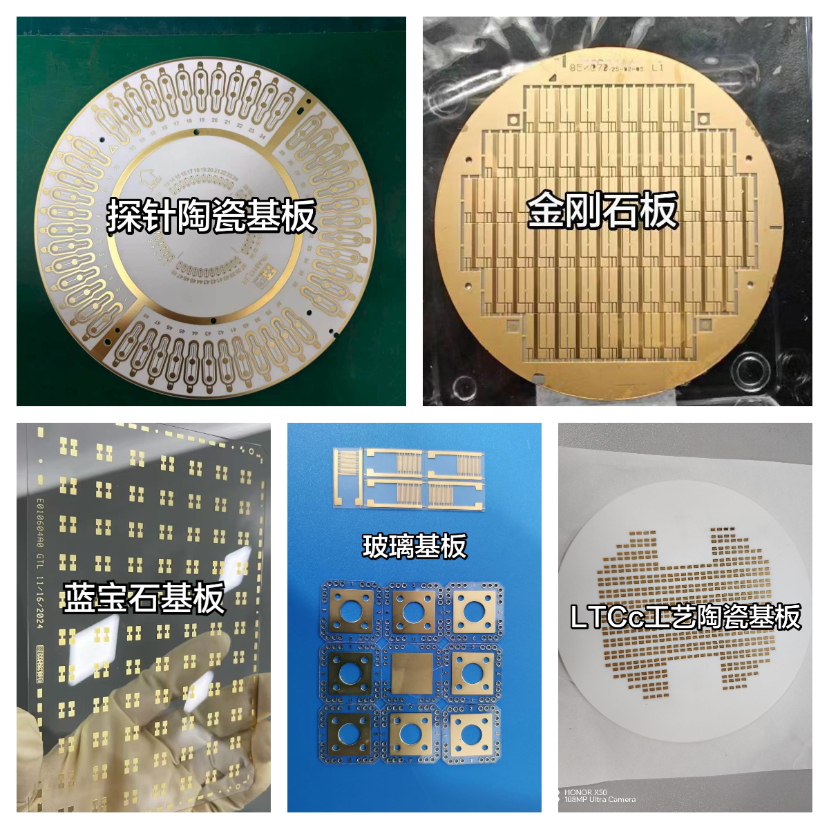
Selected Ceramic Substrate Products from Baineng Yunban
trending news
Contact Us