



Sorry, no sales person is available right now to take your call. Pls leave a message and we will reply to you via email as soon as possible.
Home/ PCB News/ 12–20 Layer High-Speed PCB Stackup Design Specification Template
12–20 Layer High-Speed PCB Stackup Design Specification Template
2026-05-12
1. Scope of Application
This stack-up design specification is developed by BaiNeng YunBoard based on years of engineering experience in high-layer-count, high-frequency, and high-speed PCB projects. It is specifically tailored for high-speed digital circuit applications and is applicable to designs involving high-speed interfaces such as DDR4/DDR5, PCIe Gen3/Gen4/Gen5, and 25Gbps+ SerDes. This specification is widely suitable for PCB design projects in communication backplanes, server motherboards, and high-end consumer electronics that demand stringent signal integrity (SI), impedance control, and electromagnetic compatibility (EMC) performance. It directly aligns with BaiNeng YunBoard’s high-precision multilayer board mass production process standards and serves as a benchmark document bridging design and manufacturing.
2. General Design Baselines
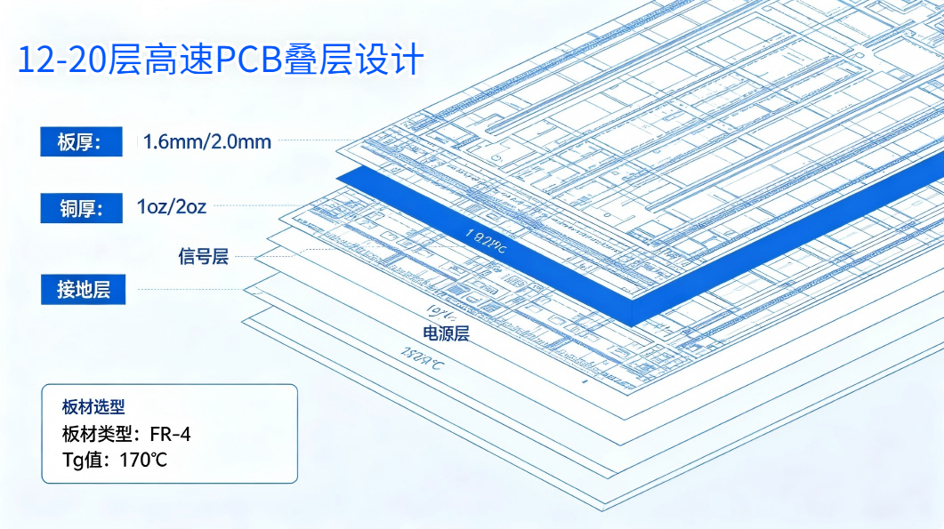
2.1 Board Thickness Standards
12-layer and 14-layer PCBs: Standard thickness is 1.6 mm.
16-layer, 18-layer, and 20-layer PCBs: Standard thickness is 2.0 mm.
For enhanced robustness, the optimized 18-layer version is recommended at 2.2 mm.
The premium 20-layer version is recommended at 2.6 mm.
All the above thickness configurations are compatible with BaiNeng YunBoard’s lamination process capabilities, effectively mitigating production risks such as warpage and interlayer misalignment in multilayer boards.
2.2 Copper Thickness Specifications
Signal layers (S): 0.5 oz (finished copper thickness approximately 0.7 mil), meeting low-loss transmission requirements for high-speed signals.
Power/Ground planes (P/G): 1.0 oz (finished copper thickness approximately 1.4 mil), ensuring sufficient current-carrying capacity and grounding integrity.
These copper thickness selections comply with BaiNeng YunBoard’s standard high-speed PCB process library, balancing signal loss, current capacity, and etching precision.
2.3 Dielectric and Material Requirements
Prepreg (PP): Uniformly use 1080 or 2116 types.
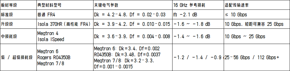
Base material selection: Materials must be selected according to signal transmission speed tiers, strictly matching loss and dielectric constant (Dk) parameters. BaiNeng YunBoard fully supports high-speed laminates ranging from standard to ultra-low-loss grades and can provide factory-measured Dk/Df parameters along with process compatibility support.
2.4 Impedance Design Baseline
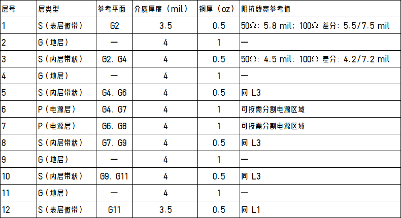
Outer-layer microstrip: Dielectric thickness of 3.5 mil, referenced to a single ground plane.
Inner-layer stripline: Referenced to dual ground planes above and below, with a total dielectric spacing of 8 mil (4 mil each side).
All impedance trace widths are theoretical calculation values. Prior to mass production, precise fine-tuning can be performed using BaiNeng YunBoard’s material parameter database and process models to ensure impedance compliance.
2.5 Layer Symbol Definitions
S: Signal layer
G: Ground plane
P: Power plane
3. High-Speed PCB Material Selection Specification
Material selection is tiered based on signal transmission speed and loss requirements to suit various high-speed application scenarios. Electrical parameter test conditions: Dk/Df @ 1 GHz / 10 GHz; loss value @ 16 GHz, 1-inch trace length. BaiNeng YunBoard supports mass customization and simulation parameter output for all grades of high-speed laminates.
4. Detailed Stack-Up Design Schemes by Layer Count
All stack-up schemes adopt a center-symmetric structure to eliminate PCB warpage risks during manufacturing and are fully compatible with BaiNeng YunBoard’s high-layer-count lamination processes. Additionally, each high-speed signal path is ensured a complete reference plane, optimizing return paths and enhancing signal integrity and EMC performance.
4.1 12-Layer PCB (6 Signal Layers, Board Thickness 1.6 mm)
Symmetry center: Between L6 and L7 (dual power planes adjacent)
Stack-up sequence: S – G – S – G – S – P – P – S – G – S – G – S
Layer allocation: 6 signal layers, 4 ground layers, 2 power layers — fully symmetric
4.2 14-Layer PCB (6 Signal Layers, Board Thickness 1.7 mm)
Design note: This scheme features an optimal symmetric structure supporting stable routing for 6 high-speed signal channels. Expanding to 8 signal layers is not recommended, as it may compromise reference plane continuity.
Symmetry center: Between L7 and L8 (dual power planes)
Stack-up sequence: S – G – S – G – S – G – P – P – G – S – G – S – G – S
Layer allocation: 6 signal layers, 6 ground layers, 2 power layers — fully symmetric
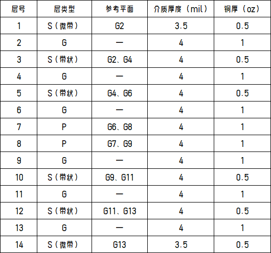
Note: Impedance parameters are identical to the 12-layer scheme. Outer-layer microstrip references L1 of the 12-layer stack-up; inner-layer stripline references L3 of the 12-layer stack-up.
4.3 16-Layer PCB (8 Signal Layers, Board Thickness 2.0 mm)
Symmetry center: Between L8 and L9 — perfectly symmetric across all layers.
Stack-up sequence: S – G – S – G – S – G – S – P – P – S – G – S – G – S – G – S
Layer allocation: 8 signal layers, 6 ground layers, 2 power layers — suitable for multi-channel high-speed routing.
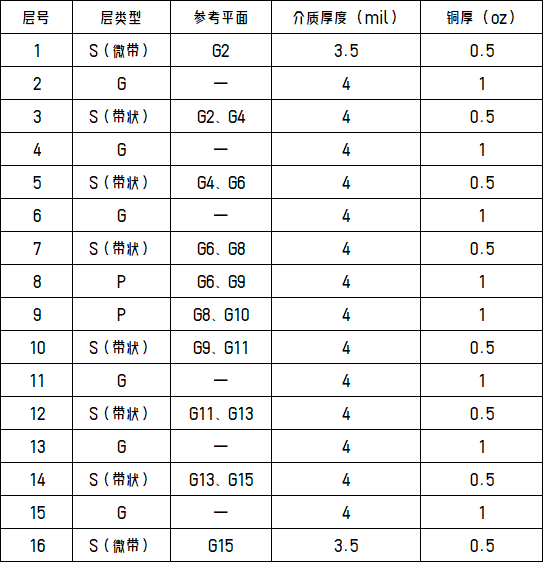
Note: Impedance parameters are identical to the 12-layer scheme.
4.4 18-Layer PCB (8 Signal Layers, Board Thickness 2.2 mm)
Design note: A mainstream, robust industry solution with ample ground layers, offering excellent shielding and return path performance. This is BaiNeng YunBoard’s recommended stack-up structure for high-frequency, high-speed applications.
Symmetry center: Between L9 and L10.
Stack-up sequence: S – G – S – G – S – G – S – G – P – P – G – S – G – S – G – S – G – S
Layer allocation: 8 signal layers, 8 ground layers, 2 power layers — significantly optimized EMC performance.
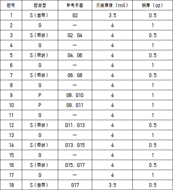
Note: Impedance parameters are identical to the 12-layer scheme.
4.5 20-Layer PCB (10 Signal Layers, Board Thickness 2.6 mm)
Design note: A symmetric solution dedicated to premium high-speed boards, supporting 10–12 signal layers while balancing routing density, signal integrity, and process stability. This is BaiNeng YunBoard’s standard high-end stack-up for computing base stations and high-end servers.
Symmetry center: Between L10 and L11.
Stack-up sequence: S – G – S – G – S – G – S – G – S – P – P – S – G – S – G – S – G – S – G – S
Layer allocation: 10 signal layers, 8 ground layers, 2 power layers.
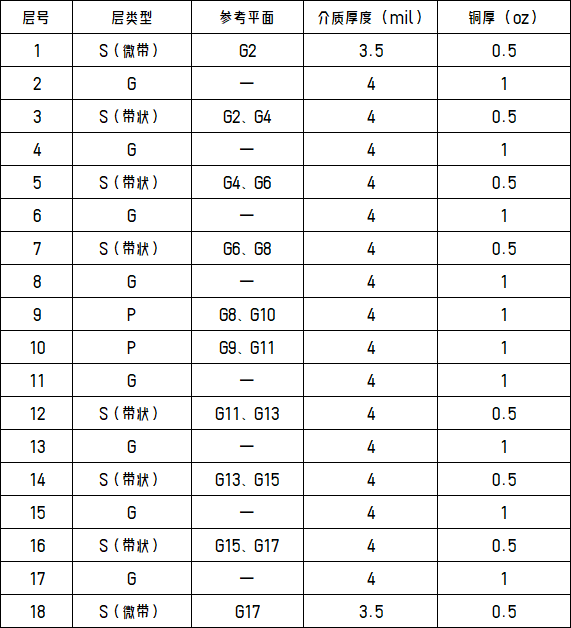
Note: Impedance parameters are identical to the 12-layer scheme.
5. Stack-Up Parameter Summary Table
The table below summarizes key parameters for each layer-count scheme, using a unified impedance baseline for quick selection. Prior to mass production, designers may submit their designs to BaiNeng YunBoard for material parameter matching and process calibration.
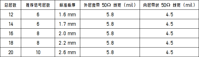
6. General Design Notes
Differential Impedance Reference
100Ω differential pairs: Microstrip line width/spacing = 5.5 mil / 7.5 mil; Stripline = 4.2 mil / 7.2 mil.
Process Compatibility Note
All impedance trace widths listed in this document are theoretical calculations. In actual production, factors such as material Dk variation, copper thickness tolerance, and etching processes may affect results. Therefore, impedance parameters must be reviewed and fine-tuned with BaiNeng YunBoard’s process engineers prior to mass production to ensure high yield.
Structural Advantages
All stack-ups employ a center-symmetric structure, effectively preventing warpage caused by thermal expansion/contraction or lamination processes. Additionally, high-speed signals are guaranteed complete reference ground planes, optimizing return paths and reducing crosstalk and EMI.
Material Matching Principle
For high-bandwidth signals such as 25 Gbps+ SerDes and PCIe Gen4/5, low-loss or ultra-low-loss materials must be used. Designers may directly select high-frequency materials from original manufacturers like Megtron or Rogers that are compatible with BaiNeng YunBoard.
For conventional high-speed signals below 10 Gbps, upgraded or standard-grade FR4 materials may be used to control costs. BaiNeng YunBoard offers cost-effective material and process solutions optimized for value.
trending news
Contact Us