



Sorry, no sales person is available right now to take your call. Pls leave a message and we will reply to you via email as soon as possible.
Home/ PCB News/ High-Frequency and High-Speed PCB Material Selection: A Professional Guide from Parameter Fundamentals to Engineering Implementation
High-Frequency and High-Speed PCB Material Selection: A Professional Guide from Parameter Fundamentals to Engineering Implementation
2026-05-11
In conventional PCB design understanding, substrate materials are often simplistically defined as physical base materials that carry circuitry and provide structural support. However, in high-speed digital circuits and microwave/millimeter-wave RF design scenarios, this perception can become a critical隐患 to product performance and reliability. PCB substrates are fundamentally core electronic components—not merely structural carriers—their material properties directly determine a device’s electrical performance, manufacturability, and long-term operational reliability.
As digital signal transmission rates continue to increase and RF operating frequencies extend into microwave and even millimeter-wave bands, the influence of PCB base material properties on system performance is magnified exponentially. Selecting materials suited to specific operating conditions ensures stable signal transmission and controllable mass production yields; conversely, incorrect material selection can trigger hidden issues such as excessive dielectric loss, signal timing drift, and impedance mismatch—leading to substandard product performance and uncontrolled manufacturing yield. This technical challenge is especially pronounced in cutting-edge fields like 5G/6G communication infrastructure, networking hardware, automotive radar, and aerospace RF systems.
Additionally, both PCB core laminates and prepreg (PP) semi-cured sheets have limited shelf lives. In engineering applications, strict adherence to the First-In-First-Out (FIFO) material management principle is essential to prevent quality issues caused by material aging, such as shifts in dielectric parameters and reduced lamination adhesion.
I. Core Understanding: High-Frequency/High-Speed Substrates Actively Determine System Performance
Modern high-frequency/high-speed PCB substrates do not possess passive support characteristics. Their key physical and electrical parameters actively participate in signal transmission, electromagnetic coupling, and thermal stress adaptation throughout system operation. Material selection must not rely on supplier recommendations or empirical practices; instead, it should be based on a structured engineering framework grounded in standards, verifiable data, and reproducible testing.
A rigorous selection methodology must be built upon IPC international industry standards, empirical validation data, and standardized test methods—this is the key to bridging the common industry gap between "perfect simulation results" and "anomalous hardware measurements." The combined merits of a substrate’s dielectric, thermal, mechanical, and conductor-matching characteristics directly define the performance ceiling of high-speed RF products.
II. Key Evaluation Dimensions for High-Speed Substrates: Comprehensive Coverage of Electrical, Conductor, Thermo-Mechanical, and Process Factors
(1) Core Electrical Parameters: Defining the Upper Limit of Signal Transmission Performance
Different core laminate and prepreg materials exhibit significant differences in electrical, mechanical, and thermal properties. Among these, dielectric constant (Dk) and dissipation factor (Df) are the two most critical parameters for high-speed/high-frequency material selection.
1. Dielectric Constant (Dk): Governing Signal Velocity, Timing, and Impedance Stability
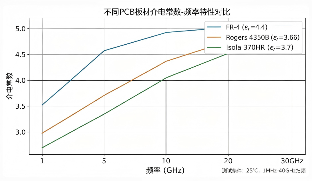
Dk is the fundamental parameter characterizing the propagation speed of electromagnetic energy through a dielectric medium. It directly determines signal transmission delay, timing alignment accuracy, and impedance consistency. Low-Dk substrates effectively enhance signal transmission speed, reduce propagation delay, and ensure timing synchronization across multi-channel serial interfaces and parallel buses—serving as a foundational requirement for high-speed digital designs.
Frequency Band Compatibility of Mainstream Substrate Materials:
Enhanced FR-4: Exhibits significant Dk variation under high-frequency conditions, with stable performance typically limited to the 3–10 GHz range—suitable only for mid-to-low frequency high-speed applications;
Hydrocarbon-Ceramic Composite Materials: Offer excellent Dk stability against temperature and frequency drift, maintaining consistent timing performance in millimeter-wave bands from 10 GHz to 30 GHz and beyond;
PTFE and Advanced Modified Materials (e.g., Panasonic M6, M7): Feature minimal Dk anisotropy and exceptional frequency stability, making them the primary choice for ultra-high-speed links like 56G-PAM4 and 112G-PAM4, as well as millimeter-wave RF designs.
A frequently overlooked factor in engineering selection is dielectric anisotropy: most PCB substrates exhibit noticeable differences in Dk values between the X-Y plane and the Z-axis direction. Using generic Dk values from datasheets in simulations without accounting for this anisotropy can lead to severe discrepancies between simulated and measured results for microstrip lines, striplines, waveguides, and resonant structures.
To ensure accurate and traceable data, Dk testing must strictly follow IPC-4101/4103 substrate specification standards and employ standardized IPC-TM-650 test methods. Using consistent data sources is essential to resolving the disconnect between simulation and physical measurement.
2. Dissipation Factor (Df): Limiting Channel Reach and Signal Integrity
If Dk governs signal speed, Df directly determines the degree of dielectric attenuation. At higher operating frequencies, dielectric loss becomes increasingly significant, directly constraining maximum channel length, eye diagram opening, and signal-to-noise ratio—effects that are particularly critical in PAM4 high-order modulation high-speed links.
Higher Df values accelerate insertion loss as frequency and transmission distance increase, drastically shortening the effective channel length in backplanes and high-density interconnect structures. In RF designs, excessive Df reduces circuit quality factor (Q) and antenna radiation efficiency, directly impairing RF system sensitivity and coverage performance.
Critical note: Df values commonly provided by suppliers are often based on single-point measurements at 1 GHz or 10 GHz. For meaningful cross-material comparisons, engineers must use standardized test conditions per IPC-TM-650. Non-standard or custom test data lacks reference value for selection and can easily lead to misjudgment.
(2) Conductor Loss Control: The Hidden Impact of Copper Foil Roughness and Surface Finish
1. High-Frequency Loss Mechanism of Copper Foil Roughness
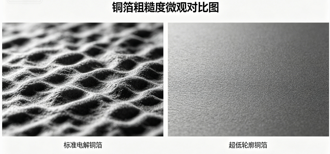
At high frequencies, the skin effect confines current flow to an extremely thin surface layer of the copper foil. Surface roughness increases the effective current path length and loop resistance, exacerbating signal attenuation. Even when paired with ultra-low-loss dielectric substrates, overall electrical performance can degrade significantly. Copper foil roughness directly impacts maximum data rate, effective channel length, RF insertion loss slope, signal phase noise, and timing jitter.
Per IPC-4562 copper foil standards, mainstream copper types include: Standard Electrodeposited (ED) copper, Very Low Profile (VLP), Hyper Very Low Profile (HVLP), and Rolled Annealed (RA) copper. VLP and HVLP foils substantially reduce high-frequency conductor loss, while RA copper offers the smoothest surface and is preferred for ultra-low-loss high-speed links and flexible circuits.
2. High-Frequency Loss Differences Among Surface Finishes
When operating frequencies exceed 2.4 GHz or trace lengths reach tens of centimeters, surface finish becomes a dominant contributor to total system loss. The nickel layer in ENIG (Electroless Nickel Immersion Gold) exhibits poor RF conductivity, introducing additional high-frequency loss. In contrast, OSP (Organic Solderability Preservative) and immersion silver finishes preserve a smooth copper surface, resulting in lower high-frequency loss and better suitability for high-speed/high-frequency signal transmission.
(3) Thermal and Mechanical Properties: Ensuring Long-Term Reliability
High-speed/high-frequency systems often operate under harsh conditions—including high temperature, thermal cycling, vibration, shock, and humidity—requiring stable electrical performance supported by robust thermal and mechanical properties. Key evaluation parameters include:
Tg (Glass Transition Temperature): Ensures structural stability of the resin system at elevated temperatures, preventing softening, deformation, and circuit failure;
Td (Decomposition Temperature): Determines the material’s ability to withstand high-temperature lead-free soldering processes—a critical indicator of manufacturing reliability;
CTE (Coefficient of Thermal Expansion): A core reliability parameter that directly mitigates via fatigue, barrel cracking, and interlayer delamination during thermal cycling.
In hybrid stack-ups combining FR-4 and PTFE, precise CTE matching between materials is essential for long-term reliability. Mismatched CTE values lead to accumulated mechanical stress, timing drift, and latent interlayer delamination failures.
Industry acceptance must strictly adhere to two key standards: IPC-6012 for rigid PCBs and IPC-6018 for RF/microwave PCBs. IPC-6018 imposes stricter requirements on dielectric uniformity, copper adhesion, and parameter consistency specifically for ultra-high-speed and high-frequency applications.
(4) Process Compatibility: The Key to Realizing Material Performance
The performance advantages of high-performance high-frequency substrates cannot be realized without precision manufacturing processes. If PCB fabricators lack experience processing specific materials, defects such as voids, rough copper surfaces, poor interlayer bonding, and dimensional inaccuracies may occur—directly negating the inherent advantages of the material.
PTFE materials impose the most stringent process requirements, necessitating customized steps: plasma or sodium etch surface activation, specialized drilling parameters, improved deburring techniques, and fusion-bond lamination processes. Process precision directly determines the structural quality of dielectric and conductive layers—making it a prerequisite for achieving target signal integrity.
During the design phase, engineers must leverage IPC-2221 and IPC-2222 DFM (Design for Manufacturability) standards to collaborate early with PCB manufacturers on stack-up optimization and process capability alignment, ensuring simulated performance translates faithfully into mass production.
III. Characteristics and Typical Applications of Mainstream High-Frequency/High-Speed Substrate Families
Based on differences in electrical performance, process complexity, and cost, mainstream high-speed substrates are clearly segmented by application:
Enhanced FR-4: Offers tighter Dk/Df control and higher Tg than standard FR-4, with excellent cost-effectiveness. Suitable for 2.5–10+ Gbps high-speed digital links and 3–6 GHz RF circuits—ideal for general-purpose mid-to-high-speed applications;
Pure PTFE Fluoropolymer Materials: Deliver ultra-low loss and stable Dk across all frequencies, but suffer from high cost and complex processing, governed by IPC-4103 standards. Primarily used in 30–100+ GHz millimeter-wave RF, radar, antennas, and ultra-high-speed digital core circuits;
Hydrocarbon-Ceramic Filled Materials: Balance low loss with good manufacturability, enabling hybrid stack-ups that overcome PTFE processing challenges. Optimally suited for 10–40 GHz RF circuits and 10–56 Gbps high-speed digital channels;
Panasonic Megtron Series: Specifically engineered for 25G/56G/112G ultra-high-speed transmission, featuring extremely low Df and excellent thermal stability, while remaining compatible with standard PCB mass production processes. Widely deployed in routers, switches, high-speed backplanes, and high-performance computing (HPC) systems.
IV. Industry Compliance Alerts: Material Regulatory Risks to Avoid
Current high-speed substrate selection faces two major regulatory risks that directly impact supply chain stability and project compliance—engineers must proactively address these during early design stages:
PFAS (Per- and Polyfluoroalkyl Substances) Restriction Risk: Most conventional PTFE substrates contain PFAS. The European Chemicals Agency (ECHA) has initiated a REACH regulation proposal to restrict PFAS across all applications, which, once implemented, could result in supply disruption and non-compliance for certain PTFE materials;
DBDPE (Decabromodiphenyl Ethane) SVHC Risk: Some Megtron series formulations contain DBDPE, which has been added to the REACH Candidate List of Substances of Very High Concern (SVHC), posing potential compliance restrictions.
Engineering teams must verify material compliance declarations early and collaborate with PCB engineering partners to identify alternative substrates that meet electrical, thermal, reliability, and regulatory requirements—thereby avoiding production halts or product non-conformance.
V. Engineering Implementation Trade-offs: Dimensional Control, Supply Chain, and Consistency Management
1. Practical Engineering Trade-offs in Material Selection
Theoretical selection must account for real-world manufacturing constraints: thinner dielectric layers improve high-speed signal performance but increase PCB warpage risk and reduce dielectric withstand voltage. Premium high-frequency substrates often face long lead times and limited inventory availability; the industry commonly uses hybrid stack-up designs to balance performance needs with supply chain realities.
Aligning material selection with the PCB manufacturer’s existing inventory during design not only shortens production lead time but also prevents batch quality issues caused by emergency material substitutions leading to parameter drift and performance variability.
2. End-to-End Consistency Control: Documentation and Collaboration Framework
Batch-to-batch and supply chain consistency are critical challenges in high-speed PCB mass production. Standardized documentation and cross-functional collaboration are essential for quality control. A complete lamination stack-up specification must explicitly state: applicable IPC standards, dielectric thickness and resin content, target Dk/Df values, IPC-4562 copper foil grade, controlled impedance specifications, IPC-TM-650 test methods, IPC acceptance criteria, and special process requirements.
Early and deep collaboration with PCB manufacturers is required to validate stack-up feasibility, impedance tolerance, CTE matching, and drilling risks—proactively preventing redesigns and performance failures. Additionally, all incoming materials must retain batch numbers and Certificates of Compliance (CoC), with full incoming inspection protocols implemented to ensure end-to-end traceability.
VI. Conclusion
In high-speed digital and RF PCB design, there is no room for compromise in substrate selection. As operating frequencies rise and design margins shrink, dielectric electrical parameters, copper quality, surface finish, and process control capabilities are deeply interconnected—collectively determining product performance and manufacturing stability.
Engineers must abandon empirical selection approaches and establish a standardized, data-driven, traceable, and manufacturable material selection system. Locking in the optimal material solution early in the project and partnering with expert PCB manufacturing teams to execute process details is the only reliable path to resolving the "simulation-passes, measurement-fails" dilemma and achieving stable performance with scalable mass production.
If you have questions regarding substrate selection for high-speed/RF projects, troubleshooting signal measurement anomalies, compliant material substitution, or high-end PCB mass production implementation, please contact the BAI NENG YunBan technical team for one-on-one customized material selection and process solutions.
trending news
Contact Us