



Sorry, no sales person is available right now to take your call. Pls leave a message and we will reply to you via email as soon as possible.
Home/ PCB News/ HDI High-Density Interconnect Printed Circuit Board Technical Specification
HDI High-Density Interconnect Printed Circuit Board Technical Specification
2026-05-09
This article provides a systematic technical exposition of High Density Interconnect Printed Circuit Boards (HDI PCBs), covering product definition, technical principles, classification by build-up layers, manufacturing processes, key parameters, product advantages, application scenarios, design guidelines, and quality control. It aims to establish a unified and standardized technical reference for HDI PCB product design, process manufacturing, incoming material inspection, quality acceptance, technical coordination, and project handover. It is applicable to hardware R&D and mass production in fields such as consumer electronics, telecommunications equipment, industrial control, intelligent automotive systems, medical electronics, and aerospace.
Product Definition and Technical Principles
Product Definition
HDI PCBs are high-density interconnect printed circuit boards manufactured using laser micro-via drilling, blind/buried via processes, plating-filled vias, and multi-layer precision lamination. Compared with traditional mechanically drilled PCBs, HDI PCBs feature micro-vias, fine traces, narrow spacing, and high interlayer integration density, enabling higher routing density and interlayer connectivity within a limited area. They serve as a critical foundational component for miniaturization, lightweighting, and high-frequency/high-speed operation of electronic devices.
Core Technical Principles
Traditional PCBs rely on large-diameter mechanical through-holes for interlayer interconnection, resulting in drawbacks such as large hole sizes, excessive space consumption, low routing density, and significant high-frequency signal loss. In contrast, HDI PCBs utilize precision laser processing to create micron-level blind and buried vias, combined with sequential lamination and plating-filled via technology, achieving a three-dimensional interconnect structure characterized by thin dielectrics, short signal paths, and high precision. This technology effectively shortens signal transmission paths, reduces transmission impedance and high-frequency crosstalk, and significantly enhances circuit integration density and signal integrity without increasing board dimensions—fully meeting the high-speed transmission demands of advanced precision electronic equipment.
HDI Build-Up Layer Classification and Process Characteristics
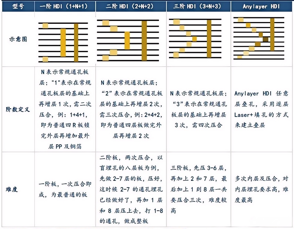
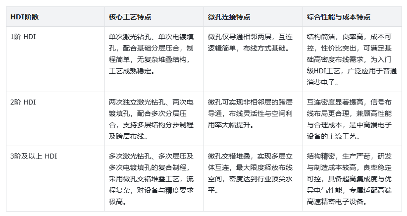
The industry typically classifies HDI PCBs into three grades—1-step, 2-step, and 3-step or higher—based primarily on the number of laser drilling cycles, plating-filled via cycles, and sequential lamination cycles. Higher step counts correspond to greater process complexity, higher routing density, and finer interlayer interconnection accuracy, enabling broader applicability in high-end scenarios. The process and performance characteristics of each grade are summarized in the table below:
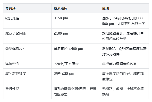
Key Technical Parameters (Industry Standards)
The following parameters are defined according to IPC-2226 industry standards and domestic HDI production norms, serving as core quantitative indicators distinguishing HDI high-density boards from traditional PCBs:
Core Manufacturing Process Flow
HDI PCBs are precision composite-process products, with core operations centered around sequential lamination, laser micro-via drilling, and plating-filled vias. Higher-step HDIs require repeated execution of these core processes. The standard production flow is as follows:
Base Material Pre-treatment: Select ultra-thin, high-heat-resistance, and high-flatness specialty base materials, followed by panel cutting, edge grinding, cleaning, and dust removal to ensure a clean, flat surface suitable for precision processing.
Inner Layer Circuit Fabrication: High-precision inner layer circuits are formed through exposure, development, etching, and resist stripping, followed by AOI inspection and defect repair.
Sequential Lamination: Based on step count and stack-up design, multiple layers are precisely aligned and pre-laminated to form a stable multi-layer foundation.
Laser Drilling: High-precision laser equipment drills blind and buried micro-vias as required, ensuring dimensional and alignment accuracy.
Plating-Filled Vias: Precision electroplating fills micro-vias, achieving metallized via walls and complete interlayer electrical connectivity, enhancing connection strength and electrical stability.
Higher-Step Repetitive Processes: For 2-step and higher HDIs, sequential lamination, laser drilling, and plating-filled via steps are repeated to construct multi-layer cross-interconnect structures.
Outer Layer Circuits and Surface Finishing: Precision outer layer circuits are fabricated, followed by solder mask application, legend screen printing, ENIG, HASL, and other surface treatments to provide corrosion resistance, oxidation protection, and solderability.
Final Inspection and Testing: Multiple tests—including AOI optical inspection, continuity testing, impedance testing, and reliability aging tests—are performed to eliminate defective units and ensure finished product quality compliance.
Core Advantages of HDI PCBs
Ultra-High Integration Density, Ideal for Miniaturized Designs
Leveraging precision processes featuring micro-vias, fine traces, and narrow spacing, HDI PCBs achieve several times the routing capacity of traditional PCBs within the same area, effectively reducing motherboard size and overall device weight. This makes them perfectly suited for slim, lightweight products such as smartphones, smart wearables, and miniature sensors.
Superior Signal Integrity for High-Frequency/High-Speed Applications
HDI’s short-path micro-via interconnect structure significantly shortens signal transmission distance, reducing signal delay, transmission loss, and high-frequency crosstalk. Its excellent electrical performance fully meets the requirements of 5G/6G communications, AI computing systems, and high-speed industrial control applications, enhancing overall system stability.
Strong Structural Stability and Long Service Life
The plating-filled via process ensures micro-vias are densely and completely filled. After multi-layer lamination, the structure becomes compact and robust, offering excellent resistance to vibration, thermal shock, and humidity/temperature aging. This effectively prevents failures such as open circuits, poor connections, delamination, and blistering during long-term use, significantly extending product lifespan and environmental adaptability.
Compatibility with Advanced High-Density Component Packaging
HDI PCBs support packaging requirements of ultra-compact, high-density surface-mount components such as BGA, CSP, and QFN, enabling high-density, fine-pitch circuit layouts. They serve as essential companion boards for high-end precision electronics, high-performance computing systems, and intelligent automotive applications.
Main Application Areas of HDI Boards
Owing to their comprehensive advantages in high density, high performance, high reliability, and miniaturization, HDI PCBs are widely used across mid-to-high-end precision electronics sectors. Key application scenarios include:
Consumer Electronics: Core motherboards for smartphones, tablets, smartwatches, wireless Bluetooth earphones, and portable wearable devices
Telecommunications Equipment: RF modules for 5G/6G base stations, communication terminal motherboards, satellite communication modules, and core cards for high-end routers
Intelligent Terminals and Industrial Control: AI computing development boards, autonomous driving vehicle control boards, industrial precision control modules, and smart security motherboards
Medical Electronics: Miniature portable diagnostic devices, high-precision testing instruments, and embedded medical control PCBs
Aerospace: Lightweight airborne control modules, precision navigation electronics, and embedded aerospace circuit assemblies
Representative Real-World Application Cases
This section presents real-world HDI PCB application cases from mass-production projects across industries, clarifying process selection, technical challenges, and implementation outcomes to vividly demonstrate the engineering value of HDI technology and provide reference for product design and process planning.
Intelligent Automotive and Industrial Control Cases
Case 1: Battery Management System (BMS) Motherboard for New Energy Vehicles
The BMS motherboard for new energy passenger vehicle power battery systems is a flagship mass-production solution from Baineng Yunban, utilizing a 12-layer 2-step HDI PCB, specifically engineered to address the challenge of integrating high-density signal acquisition with high-current power delivery on automotive motherboards. Baineng Yunban optimized the multi-layer 3D routing structure to support over 2,000 high-precision monitoring points for battery temperature, voltage, and current, reducing signal delay by 40% for real-time, accurate data acquisition. The power region employs a multi-via parallel buried-via design to precisely control current density, keeping overall temperature rise below 10°C and reducing system failure rates to 0.1‰—fully compliant with automotive Grade A reliability standards and suitable for complex automotive environments involving vibration and wide temperature swings. The solution has been mass-produced for multiple leading new energy vehicle manufacturers.
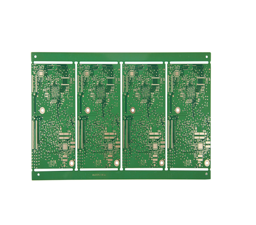
12-Layer 2-Step HDI Board
Case 2: ADAS Perception Board for Autonomous Driving
The integrated millimeter-wave radar and vision perception board for Advanced Driver Assistance Systems (ADAS) was custom-developed and mass-produced by Baineng Yunban using an 8-layer 2-step HDI process. Addressing the stringent requirements of automotive high-precision perception systems for signal real-time performance and operational stability, Baineng Yunban leveraged mature HDI fine-pitch impedance-matched routing and micro-via short-path interconnect technology to effectively suppress high-frequency crosstalk, ensuring precise radar ranging and image transmission. The board reliably operates in automotive-grade -40°C to +85°C wide-temperature environments, resolving traditional PCB limitations such as sparse routing, high signal delay, and weak interference immunity. It serves as an excellent companion solution for high-level autonomous driving perception systems and has achieved mass production in OEM automotive programs.
8-Layer 2-Step HDI Board
Medical Electronics Case
Case: Motherboard for Portable Ultrasound Diagnostic Device
The core motherboard for a high-end portable medical ultrasound device was developed and manufactured by Baineng Yunban, featuring a 12-layer 3-step HDI blind/buried via structure paired with low-loss high-frequency specialty laminate. Traditional PCBs often suffer from insufficient routing density and severe signal interference, leading to image transmission delays and blurry imaging.
Baineng Yunban optimized the HDI stack-up and micro-via layout, shortening critical signal paths by 20% and limiting high-frequency crosstalk to ≤ -60 dB, resulting in a 35% improvement in imaging speed and significantly enhanced resolution. Additionally, leveraging HDI’s high-density integration advantage, the motherboard volume was reduced by 40%, enabling a lightweight, portable device design that fully complies with high-reliability and high-stability standards for medical equipment. It is now widely deployed in clinical mobile diagnostic applications.
12-Layer 3-Step HDI Board
Aerospace and Defense Case
Case: High-Frequency Control Board for Military Lightweight UAV
The airborne control and radar module PCB for military reconnaissance drones is a custom high-step HDI product from Baineng Yunban, strictly manufactured in accordance with MIL-PRF-31032 military standards. Addressing the drone’s core requirements for lightweighting, low observability, and high-precision signal transmission, Baineng Yunban employed ultra-high-density HDI routing to significantly reduce board size and weight, fitting confined airborne installation spaces. Through stacked micro-via interconnects and proprietary anti-interference process optimization, the board enables lossless transmission of 10 GHz radar signals, delivering excellent electromagnetic interference resistance and thermal shock resilience—ensuring long-term stable operation in high-altitude, high-speed, and complex electromagnetic environments. It stands as a premium companion solution for military lightweight airborne systems.
Design Guidelines and Quality Control Standards
Key Design Guidelines
1. Strictly align stack-up design with HDI step count to avoid micro-via overlap and trace conflicts, ensuring lamination alignment accuracy and structural rationality.
2. Maintain a minimum annular ring width of 50 μm around micro-vias to enhance plating-filled via stability and interlayer structural strength, preventing via cracking or detachment.
3. Route high-speed signals independently with proper impedance matching to avoid high-frequency crosstalk and signal attenuation, ensuring signal integrity.
4. Deliver standard Gerber or ODB++ manufacturing files, clearly specifying step count, via-filling process, stack-up parameters, and test standards.
Finished Product Quality Acceptance Criteria
Appearance: Clean board surface free of oxidation, scratches, exposed copper, or stains; uniform and full solder mask; clear and accurate legend markings.
Electrical Performance: All traces and micro-vias exhibit normal conductivity with no shorts, opens, or abnormal resistance; stable electrical performance.
Process Quality: Plating-filled vias are fully filled with no voids or dimples; lamination structure shows no delamination, blistering, or misalignment.
Reliability: Passes thermal cycling, humidity/temperature aging, and mechanical vibration tests with no performance degradation or structural damage post-test.
Industry Development Trends
As the electronics industry continues evolving toward miniaturization, high frequency, high speed, and high integration, traditional PCBs increasingly fail to meet the demands of advanced equipment. Consequently, market penetration of high-step HDI PCBs is steadily rising. Currently, China is making continuous breakthroughs in core HDI technologies—including manufacturing processes, laser drilling, and precision lamination—gradually achieving domestic substitution for high-end, high-step HDI products. With the rapid growth of emerging industries such as 6G communications, artificial intelligence, intelligent vehicles, low-altitude economy, and high-end medical devices, HDI PCBs will continue advancing toward higher precision, higher step counts, lower transmission loss, better thermal management, and enhanced reliability.
Conclusion
HDI high-density interconnect printed circuit boards are fundamental components of modern precision electronics. Compared with traditional PCBs, they offer core advantages including high routing density, superior electrical performance, structural stability, and broad applicability. Different HDI step configurations correspond to varying levels of process complexity, cost ranges, and performance tiers, enabling precise alignment with product requirements in high-end sectors such as industrial control, automotive, medical electronics, and aerospace. The multi-industry implementation cases from Baineng Yunban presented in this chapter fully validate HDI technology’s core value in device miniaturization, high-speed signal transmission, and reliable operation under complex conditions. Against the backdrop of continuous electronic device advancement and accelerated domestication of high-end hardware, HDI process technology will keep innovating and iterating, providing solid process support and production capacity assurance for the high-quality development of China’s advanced precision electronics industry.
trending news
Contact Us