



Sorry, no sales person is available right now to take your call. Pls leave a message and we will reply to you via email as soon as possible.
Home/ PCB News/ Special Processes in Package Substrate Manufacturing: Coreless Process and Embedded Circuit Process Technology Analysis
Special Processes in Package Substrate Manufacturing: Coreless Process and Embedded Circuit Process Technology Analysis
2026-04-20
In the field of IC substrate manufacturing, subtractive (Tenting), modified semi-additive process (mSAP), and semi-additive process (SAP) constitute the three mainstream process technologies. Meanwhile, specialized processes such as coreless technology, embedded trace substrate (ETS, also known as Embedded Pattern Process), and via-post coreless are gradually becoming key complementary technologies in advanced packaging. These processes precisely meet the stringent requirements of cutting-edge applications—including AI computing, low-earth-orbit satellites, and intelligent cockpits—for package substrates, thanks to their unique advantages in structural design, wiring density, electrical performance, and thinness. They also represent critical technological frontiers that must be overcome in China’s ongoing efforts toward IC substrate localization. This article focuses on coreless technology and its derivative—embedded trace substrate (ETS)—and systematically elaborates their process principles, core advantages, and applicable scenarios based on the latest technical advancements.
1. Coreless Substrate Technology
Coreless substrate technology was first introduced by Fujitsu in 2006, formally known as Coreless Package Substrate. This technology eliminates the rigid core layer traditionally used in organic substrates, relying entirely on high-density build-up layers to achieve extreme thinness and miniaturization—addressing the demanding requirements of advanced chips for reduced dimensions and low signal loss at high frequencies.
Compared with conventional core-based organic substrates, the fundamental distinction of coreless substrates lies in the complete absence of a rigid core layer; all conductive layers are formed through build-up structures without mechanical support from a core. Key characteristics include ultra-thin profiles, low dielectric constant (Low Dk), and low dissipation factor (Low Df), offering significant advantages in high-frequency and high-speed transmission scenarios. Coreless substrates have been widely adopted in high-end logic chips (AP), memory chips, RF chips, and MEMS devices. Several domestic enterprises have already achieved mass production of coreless substrates and successfully entered the supply chains of well-known chip design companies.
2. Embedded Trace Substrate (ETS / EPP) Technology
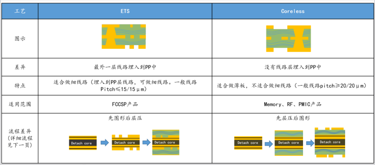
ETS, also known as embedded circuit substrate technology, is characterized by circuit patterns that are flush with the surface of the prepreg (PP) layer—hence the term “flush substrate.” Developed as an advanced evolution of the coreless architecture, ETS is regarded as one of the pivotal technologies for breaking through high-end substrate barriers and securing leadership in intelligent computing-era packaging.
Process Principle: ETS utilizes a detachable carrier (Detach Core) to form embedded circuit patterns. The process begins with precisely fabricating circuit patterns on the surface of the detachable carrier via pattern plating or other methods. Next, lamination bonds the prepreg (PP) tightly onto the carrier-mounted circuits, fully embedding the traces within the dielectric layer. After lamination and panel separation, the base copper of the carrier is removed by etching, leaving behind conductive patterns embedded inside the dielectric. This approach effectively ensures fine feature resolution and excellent surface planarity.
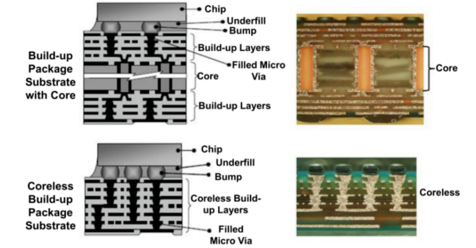
Advantages over mSAP:
Superior fine-pitch capability: Since ETS traces are fully embedded within the PP dielectric, they avoid lateral etching—a common issue in traditional semi-additive processes that causes line-width loss—enabling smaller line/space (L/S) dimensions.
Exceptional thinness: Supported by the stable Detach Core, ETS allows precise control over total thickness, easily meeting ultra-thin packaging demands—particularly suitable for AI accelerator cards and advanced system-in-package (SiP) products.
In ETS structures, circuit patterns are embedded within the insulating dielectric layer. Combined with the coreless architecture, this enables fine-feature circuits without additional cost and significantly simplifies layer reduction—for example, readily optimizing a 4-layer design down to 3 layers. Because etching is independent of pattern width, line dimensions can be precisely controlled. Thus, ETS has become the preferred method for mass-producing fine lines with L/S < 12μm. As of 2026, the industry’s smallest demonstrated ETS L/S is 5/5μm; Chinese manufacturers have stably mass-produced 15/15μm, with leading firms capable of achieving 12/12μm.
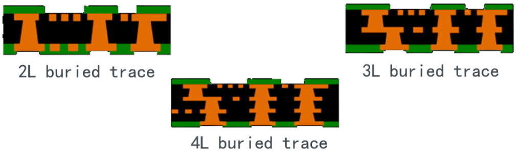
Currently, ETS technology is primarily used to construct a single circuit layer in 2-, 3-, or 4-layer substrates, and can be further extended into vertically stacked multi-layer ETS patterns to meet higher integration density requirements. It should be noted that ETS traces differ fundamentally in morphology from those made by sequential build-up SAP: ETS traces are fully embedded within the dielectric layer of the copper-clad laminate (CCL), whereas SAP traces sit atop the dielectric layer. However, both exhibit rectangular cross-sections, which enhance signal integrity and suit high-frequency, high-speed packaging applications.
3. Two Implementation Methods of ETS
1. Pattern Plating Approach
This method uses a detachable carrier (Detach Core) as the foundational support for fine-line fabrication. Typically, thin dry film (<25μm) defines fine patterns, with copper thickness controlled at 10–15μm. After lamination and panel separation, the pattern is transferred into the prepreg, followed by base copper removal via etching. Blind vias are usually formed by laser ablation from the opposite side of the embedded layer. Since PP material is resin-rich, it effectively shields copper traces from direct contact with glass fibers, preventing conductive anodic filament (CAF) defects and significantly enhancing reliability. This is currently the most widely adopted industrial approach, with Chinese companies such as Guangxin Substrate, Fastprint, Unimicron, Ample Solutions, and Hongban Tech already achieving mass production.
2. Laser Trenching Approach
This method starts with a standard core substrate. Circuit patterns are first formed on one side, while the opposite side undergoes precise laser ablation to create high-density trenches with fine pitch, along with blind vias. A specialized plating process then deposits metal preferentially into trenches and vias across the entire ETS surface, minimizing excess copper that would later require flash etching—thus reducing process loss. However, laser patterning is relatively slow compared to laser direct imaging (LDI), limiting throughput. Additionally, any non-uniform ablation (e.g., inconsistent depth) may introduce latent defects in the final product. Consequently, this method is less commonly used than pattern plating.
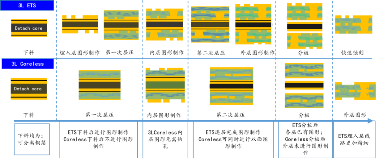
4. Comparative Analysis and Industry Adoption of Coreless vs. ETS
It should be emphasized that all coreless processes described above rely on a detachable carrier (Detach Core). Detach Core is an ultra-thin copper foil core fabricated via reverse lamination, with peel strength precisely controlled by an interfacial release layer. Release layers fall into two main categories: organic and inorganic binders. Inorganic binders offer tunable peel strength, making them highly adaptable to diverse production needs and a key focus of domestic technological development.
Globally, in the first three quarters of 2024, IC substrate market share was dominated by manufacturers from Taiwan, South Korea, and Japan, collectively accounting for 86.2%, while mainland Chinese firms held only 8.3%—highlighting urgent and substantial demand for localization. Coreless and ETS technologies, as critical pathways to overcoming traditional packaging substrate limitations, not only enable ultra-thin, high-precision products but also reduce manufacturing complexity and enhance reliability through detachable carrier design. While coreless technology excels in overall thinness and low-loss electrical performance, ETS stands out in embedded fine-line fabrication, surface planarity, and fine-pitch capability. Together, they form a core technological matrix empowering Chinese enterprises to breach high-end substrate barriers and accelerate domestic substitution—laying a solid foundation for the industry’s high-end transformation and future process optimization for emerging applications.
trending news
Contact Us