




Sorry, no sales person is available right now to take your call. Pls leave a message and we will reply to you via email as soon as possible.
Home/ PCB News/ Applications and Advantages of Microvias in Modern PCB and HDI Designs
Applications and Advantages of Microvias in Modern PCB and HDI Designs
2026-04-17
Microvias are a core feature in modern printed circuit board (PCB) design, and their importance is increasingly evident—particularly in the field of high-density interconnect (HDI) technology. These miniature conductive vias, formed via laser processing, efficiently enable interconnections between copper traces across PCB layers, providing critical technical support for the miniaturization and high-speed operation of electronic devices. This article systematically explores the structural characteristics of various via types in PCBs, the key advantages of microvias, and their essential roles in enhancing signal integrity, power integrity, and thermal management performance.
1. Overview of Vias in PCB Design
Vias, or Vertical Interconnect Accesses (VIAs), are conductive pathways in PCBs that provide both electrical and mechanical connections between different layers. Essentially, a via is a hole plated with conductive metal on its inner walls; it may be filled or left hollow based on design requirements. Its primary function is to connect one or more layers of copper foil within a multilayer PCB stack-up, enabling signal, power, or ground paths to traverse between layers.
Vias are primarily categorized into three types based on their structure and location:
Through-hole vias: Extend from the top layer through to the bottom layer of the PCB, connecting all internal copper layers. This is the most traditional and fundamental via type.
Blind vias: Drilled from an outer layer and terminate at a specific internal layer, connecting only the outer layer to the designated inner layer without penetrating the entire board thickness.
Buried vias: Entirely embedded between internal layers of the PCB, not extending to any outer surface and thus invisible externally. They are used exclusively for interconnections between inner layers.
Traditional vias are typically fabricated using mechanical drilling followed by copper plating to form conductive pathways. This method is mature and highly reliable, and remains widely used today. However, in high-density PCB layouts, the limitations of mechanically drilled vias have become increasingly apparent, primarily in the following three aspects:
Large footprint: Traditional vias have relatively large diameters, occupying valuable routing space, complicating compact layout design, and limiting PCB integration density.
Poor signal integrity: The metallic barrel structure of vias introduces parasitic capacitance and inductance, causing signal reflections and impedance discontinuities that degrade high-speed signal transmission quality.
Inadequate mechanical reliability: In deep, high-aspect-ratio traditional vias, voids, cracks, and other defects can easily occur during electroplating, reducing the PCB’s mechanical strength and service life.
2. The Critical Role of Microvias in HDI PCB Design
One of the core advantages of HDI technology is its effective resolution of the challenges posed by traditional vias in high-density designs through the use of microvias. Fabricated using laser drilling, microvias are small, shallow holes with depths typically less than 0.25 mm. Thanks to their unique structural characteristics, microvias offer the following significant benefits:
Compact size: Microvias have much smaller diameters than traditional vias, enabling compatibility with high-speed, fine-pitch components, significantly increasing PCB integration density, and meeting the design demands of miniaturized electronic devices.
Enhanced signal integrity: Compared to traditional vias, microvias exhibit substantially reduced parasitic capacitance and inductance, effectively minimizing signal reflections and crosstalk to ensure stable high-speed signal transmission.
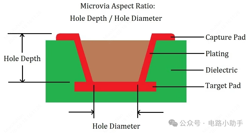
Higher reliability: Microvias have low aspect ratios (typically 0.6:1 to 1:1), making them less prone to defects during plating and resulting in more consistent and stable plating quality, thereby improving overall PCB reliability.
Figure 1: Schematic illustration of microvia structure (showing depth-to-diameter relationship)
The aspect ratio of microvias ranges from 0.6:1 to 1:1, with diameters between 50–250 μm.
3. Common Microvia Configurations
High-speed digital (HSD) design continues to push PCB density to its limits. Core components such as application-specific integrated circuits (ASICs) and field-programmable gate arrays (FPGAs) often employ chip-scale packages (CSP), ball grid arrays (BGAs), or micro-ball grid arrays (μBGAs) with over 1,000 pins. Routing these components requires carefully designed fanout structures to route I/O pins from central pads into inner PCB layers while maintaining uniform trace distribution and minimum trace width to avoid signal interference.
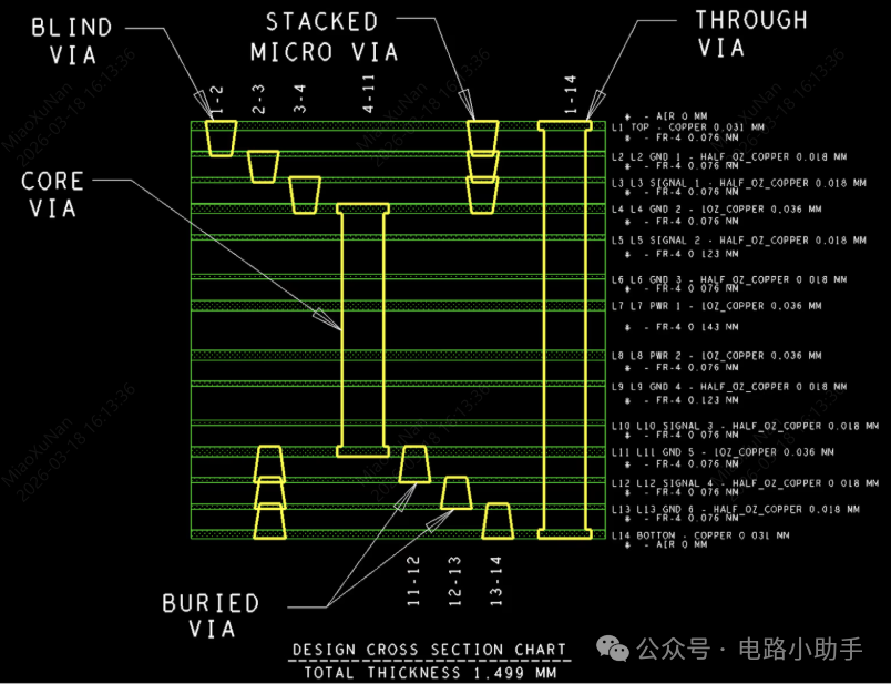
As shown in Figure 2, in HDI designs, microvias are typically configured in either stacked or staggered arrangements, commonly found in 3+N+3 and more complex multilayer structures:
Stacked microvias: Multiple microvias are vertically aligned and must be filled with conductive material and capped to ensure stable and reliable interlayer connectivity.
Staggered microvias: Multiple microvias are offset from one another and can achieve interlayer conduction without filling or capping, simplifying the manufacturing process.
It is important to note that in fanout routing for fine-pitch, high-pin-count integrated circuits (ICs), the arrangement of microvias and the placement of blind and buried vias are critical. Asymmetric stacking of microvias can cause uneven stress during PCB fabrication, leading to board warpage and other quality issues that affect subsequent component soldering and overall performance.
Figure 2: Schematic of a 14-layer 3+N+3 PCB structure, clearly illustrating stacked and staggered microvia configurations.
4. Enhancing Signal Integrity with Microvias
In high-speed digital designs, radio-frequency energy generated during signal transmission can cause various signal integrity issues, even producing harmonic interference extending into the millimeter-wave range. Any branched signal path can act as a stub, resonating within the HSD operating bandwidth and causing destructive interference and signal power loss at resonant frequencies. If this power loss occurs in regions of high signal energy, it distorts the waveform and increases bit error rate (BER), impairing device functionality. Therefore, shortening via length and minimizing interference along signal paths are crucial for improving signal integrity.
Microvias implemented as blind or buried vias meet this requirement perfectly—their shorter length compared to traditional through-hole vias results in superior electrical performance and significantly reduced self-inductance. However, the low aspect ratio of microvias requires HDI outer layers to use thin substrates (~60 μm thick). Under these conditions, achieving a standard 50 Ω impedance necessitates extremely narrow trace widths, as transmission line impedance depends primarily on dielectric thickness, dielectric constant, trace width, and spacing. Conversely, wider traces can be used for inner-layer transmission lines, reducing loop self-inductance and overall transmission line inductance to further enhance signal integrity.
5. Improving Power Integrity with Via-in-Pad (VIP) Microvias
Via-in-Pad (VIP) microvia technology directly connects IC landing pads to inner PCB layers, effectively enhancing power integrity. Its advantages are reflected in two key areas:
Reduced parasitic inductance: VIP microvias shorten current loops, improving power decoupling and reducing power supply noise.
Improved transient response: Capacitors can respond more quickly and effectively to transient current demands, ensuring stable power delivery (as shown in Figure 3).
Compared to standard through-hole VIPs, microvia VIPs can reduce parasitic inductance and capacitance by up to 90%, significantly optimizing power integrity and providing reliable support for the stable operation of high-speed, high-power electronic devices.
Figure 3: Schematic of PCB pad mounting using VIP technology to connect power and ground planes.
6. Addressing Soldering Challenges with VIP Microvias
Despite their significant advantages, VIP microvias can lead to soldering issues if improperly designed or processed. The most common problem is solder wicking—capillary action draws molten solder through the microvia opening into the PCB interior, resulting in insufficient solder on the pad. Whether the microvia is located on or near the pad, effective measures must be taken to prevent solder loss; otherwise, open circuits, short circuits, component tombstoning, or interference with adjacent components may occur. Therefore, VIP microvia design must strictly control aperture size and position and incorporate appropriate filling or capping processes to avoid soldering defects.
7. The Role of Microvias in Thermal Management
Thermal management is an indispensable aspect of HDI design. Due to the dense component placement on HDI PCBs and the mismatch in coefficients of thermal expansion (CTE) between materials (e.g., dielectric layers and copper foil), thermal stress generated during operation can lead to serious issues: not only causing mechanical failures such as microvia interface cracking and PCB delamination, but also triggering electrical performance degradation that compromises device reliability and lifespan.
The primary goal of thermal management is to efficiently transfer heat away from hotspots to reduce thermally induced failure risks. In many HDI designs, microvias play this critical role—by providing direct thermal pathways from large ground pins (commonly found in the center regions of quad flat pack (QFP) devices) to inner PCB layers, they rapidly conduct heat generated by components to internal heat-spreading structures, enabling more efficient heat dissipation and mitigating the adverse effects of thermal stress.
8. Common Microvia Failure Modes and Prevention Strategies
The primary cause of microvia failure is Z-axis thermal expansion—differences in CTE between PCB dielectric layers and copper foil generate stress during temperature changes, leading to microvia damage. Secondary causes include inconsistent design files (Gerber data) and manufacturing defects (e.g., plating voids, copper separation).
Common microvia failure modes in PCB design and manufacturing include:
Misalignment (offset) between microvia and target pad
Cracks in microvia barrel walls or corners
Interlayer misregistration (alignment errors)
Target pad pull-away
Voids in copper plating or separation between copper cap and via wall
To address these failure modes, designers and manufacturers can implement optimized design practices (e.g., appropriate aspect ratio control, precise interlayer alignment), standardized manufacturing processes (e.g., improved plating quality, strict thermal parameter control), robust design-for-manufacturability (DFM) reviews, and thermal sensitivity testing to effectively prevent microvia failures and enhance PCB reliability.
9. Conclusion: The Core Value of Microvias in Modern PCB Design
Microvias are the cornerstone of contemporary HDI PCB design. With their compact size, excellent electrical performance, and reliable structural characteristics, microvias enable high-density fanout routing, cleaner signal paths, more compact power loops, and more efficient thermal pathways—perfectly aligning with the industry trends toward miniaturization, high speed, and high integration in electronic devices.
By strategically employing blind vias, buried vias, and via-in-pad (VIP) microvia structures, designers can minimize parasitic effects, reduce bit error rates (BER), enhance power decoupling performance, and improve overall PCB reliability. However, successful implementation of microvia technology hinges on meticulous attention to detail: balancing microvia stacking methods, selecting appropriate aspect ratios, standardizing fill/cap processes, and rigorously conducting DFM reviews and thermal sensitivity tests are essential to effectively mitigate Z-axis thermal stress and plating defects, ensuring optimal PCB design performance and manufacturing quality.
trending news
Contact Us