



Sorry, no sales person is available right now to take your call. Pls leave a message and we will reply to you via email as soon as possible.
Home/ PCB News/ A Complete Guide to PCB Embedded Copper Block Boards: Specialized Circuit Boards for Heat Dissipation and High Current
A Complete Guide to PCB Embedded Copper Block Boards: Specialized Circuit Boards for Heat Dissipation and High Current
2026-03-20
1. Core Definition of PCB Embedded Copper Block Boards
PCB embedded copper block boards are specially customized printed circuit boards. The core process involves embedding solid copper blocks of specific shapes into internal PCB layers or pre-machined cavities, securing them with thermally conductive insulating materials, and then laminating the entire assembly into a single integrated structure. This design specifically addresses industry pain points such as heat dissipation challenges in high-power circuits and unstable high-current transmission.
Compared to conventional PCBs that rely solely on copper traces for conduction and heat dissipation, embedded copper block boards fundamentally differ across three dimensions: structure, functionality, and manufacturing process:
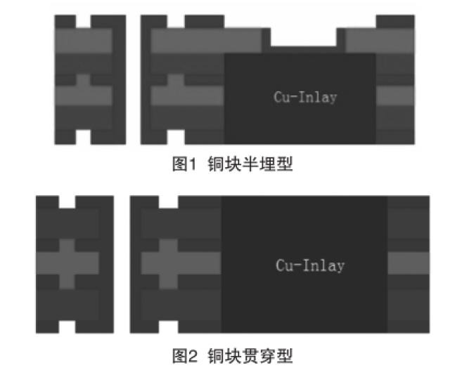
Structural Aspect: It breaks the limitation of standard PCBs, which only have thin copper traces, by embedding three-dimensional solid copper blocks to create an integrated thermal and electrical conduction structure—no longer relying solely on thin surface traces for heat dissipation and current conduction;
Functional Aspect: It serves two primary purposes simultaneously—it acts as a highly efficient heat dissipation channel for high-power electronic components, rapidly removing heat; and leverages copper’s low resistivity to serve as a dedicated high-current transmission path;
Process Aspect: This is a non-standard, specialized PCB manufacturing technique. It requires precisely milling cavities before lamination and embedding copper blocks, with particular focus on resolving issues like mismatched coefficients of thermal expansion (CTE) between copper and FR4 substrates, insufficient bonding strength, and excessive internal stress. The process complexity far exceeds that of standard PCB production.
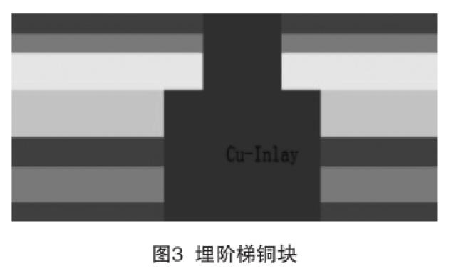
2. Core Intent and Practical Value of Embedded Copper Block Design
The design of embedded copper blocks is not merely a structural improvement but a targeted solution to industry challenges in high-power, high-stress, and high-current applications. Its core benefits focus on four key dimensions:
1. Efficient Heat Dissipation and Uniform Temperature Distribution
Copper conducts heat significantly faster than standard PCB substrates like FR4. Solid copper blocks rapidly dissipate localized high temperatures generated by high-power components, creating low thermal resistance paths to transfer heat to the PCB surface or external heat sinks. This effectively eliminates hotspots and ensures long-term component reliability, offering a highly effective passive cooling solution beyond air or liquid cooling.
2. Significantly Enhanced High-Current Carrying Capacity
Copper blocks exhibit extremely low electrical resistance, easily handling currents exceeding tens of amperes. Their combined electrical and thermal performance far surpasses that of standard thick-copper PCBs, preventing issues like trace overheating and excessive voltage drop. This makes them ideal for high-current applications such as power modules, power devices, and LED drivers.
3. Enhanced Mechanical Structural Strength of PCB
At locations prone to mechanical damage—such as connector mounting areas, regions subject to repeated insertion/extraction, or board edges—the embedded copper blocks act like "reinforcing rivets," increasing local board hardness. This effectively resists deformation from external impacts or repeated mechanical stress, preventing structural failures like cracking or delamination.
4. Creation of Dedicated Low-Thermal-Resistance Pathways
For components with stringent thermal requirements—such as high-power LEDs, RF power amplifiers, and power semiconductors—the embedded copper block can be directly bonded to the component’s heat-generating surface, establishing the shortest possible low-thermal-resistance path. This dramatically improves heat dissipation efficiency and extends component lifespan.
3. Core Process Characteristics and Manufacturing Challenges of Embedded Copper Block Boards
The embedded copper process deviates entirely from standard PCB manufacturing flows. Key challenges center on precision encapsulation, positioning control, and lamination reliability, requiring meticulous attention throughout production to mitigate quality risks:
1. Precision Slot Milling and Filler Material Selection
Using CNC milling, cavities matching the exact dimensions of the copper blocks are machined into inner core layers with extremely tight tolerances. The gap between the copper block and cavity wall must be completely filled with high-thermal-conductivity prepreg or specialized thermal adhesive—ensuring both efficient heat transfer and stress buffering against CTE mismatch between copper and substrate, while eliminating voids or air bubbles.
2. Resin Flow and Positioning Control During Lamination
Solid copper blocks have high heat capacity and absorb significant heat during lamination, often disrupting normal resin flow and leading to incomplete filling. This requires tailored adjustments to lamination temperature, pressure, and duration, along with added resin flow channels to manage excess resin. Simultaneously, high-temperature tapes or etched alignment slots are used to temporarily fix copper blocks, preventing displacement and ensuring precise placement.
3. Reliability Risk Mitigation
The large difference in CTE between copper and PCB substrates can easily cause warpage, delamination, or cracking if design or process controls are inadequate. Subsequent mechanical drilling must strictly avoid copper blocks to prevent drill breakage; thus, irregular or precision holes are typically drilled using lasers, or process holes are pre-machined into the copper blocks.
4. Basic Parameters and Process Capabilities of Embedded Copper Block Boards
The manufacturability of embedded copper block boards directly determines product applicability, with core parameters, tolerances, and performance requirements adhering to established industry standards:
1. Copper Block Specifications
Thickness Range: Typically controlled between 0.5mm and 3.0mm, customizable based on thermal and current requirements;
Planar Dimensions: Common sizes range from 3×3 mm to 40×100 mm; oversized blocks require optimized lamination processes.
2. Copper Block Structural Shapes
Various custom shapes can be fabricated to meet different bonding and mounting needs. Mainstream configurations include:
Type I (Rectangular/Square): Basic form, simple to manufacture, most widely used;
Type T (Undercut): Features an undercut protrusion that significantly enhances bonding strength with the substrate, preventing detachment;
Type U (Slotted): Designed for edge mounting or clearance scenarios, offering flexible layout adaptation.
3. Core Precision Controls
Processing precision is critical in embedded copper technology, directly affecting risks of short circuits and SMT assembly yield:
Clearance: Minimum distance from copper block edges to traces or holes ≥ 0.25mm–0.35mm to fully eliminate short-circuit risks;
Flatness: Height difference between copper block surface and PCB surface controlled within ±30µm – ±50µm to ensure high SMT yield.
4. Performance Validation Requirements
Finished products must pass rigorous high-potential (Hi-Pot) tests, high-current load tests, and thermal cycling tests to guarantee long-term stable operation under high voltage, high current, and repeated thermal cycling—without failures such as leakage, overheating, or delamination.
5. Standard Classification System for Embedded Copper Block Boards
There is no universal classification standard for PCB embedded copper block boards. The industry primarily categorizes them based on copper block embedding structure, copper block shape, and base substrate material. Different types vary significantly in application scenarios and process focus:
1. Classification by Structural Configuration (Based on Copper Block Placement)
Blind Embedded: Copper block does not penetrate through the PCB—exposed on one side and embedded internally on the other—ideal for directional heat conduction and applications requiring a flat backside;
Through-Embedded (Straight Copper Block): Copper block fully penetrates the PCB, exposed on both top and bottom surfaces, creating a through-hole thermal path—ideal for transferring heat from front-side components directly to rear-mounted heat sinks;
Stepped Through-Embedded (Stepped Copper): Features a stepped cross-section with gradually varying area, maximizing heat dissipation within confined spaces—suitable for specialized mounting structures;
Fully Internal Embedded: Copper block is completely enclosed within the PCB with no surface exposure—ideal for internal thermal equalization, localized high-current conduction, and designs demanding exceptional surface flatness.
2. Classification by Copper Block Shape (Based on Process Complexity)
Type I: Standard rectangle—simple process, low cost, highly versatile;
Type U: Features a slotted structure—suited for clearance or edge mounting—requires higher machining precision;
Type T: Undercut anti-detachment design—offers superior bonding strength—but involves complex processing and stringent alignment requirements.
3. Classification by Base Substrate Material (Based on Process Focus)
FR4 Embedded Copper Block Boards: Most common type, moderate cost—key challenge lies in addressing CTE mismatch and insufficient adhesion between copper and FR4 epoxy resin;
High-Frequency Hybrid Laminate Embedded Copper Block Boards: Copper blocks embedded into high-frequency substrates like RO4003C—balancing RF/microwave signal integrity with power amplifier thermal management. This demands strict control over dimensional stability consistency between different substrate materials due to high process complexity.
6. Standard Manufacturing Workflow for Embedded Copper Block Boards
The core workflow is consistent across all embedded copper block board types, with variations mainly in pre-lamination slot preparation and copper block shaping. The standard process is as follows:
Material Preparation and Inner Layer Processing: Core sheets and prepregs are cut to size; inner layer circuitry is fabricated; solid copper blocks of matching specifications are prepared;
Precision Slot Milling: CNC milling creates copper block cavities in core layers and prepregs, ensuring dimensional and positional tolerances meet specifications;
Copper Block Oxide (Brown Oxide) Treatment: Copper block surfaces undergo brown oxide treatment to create micro-roughness, significantly enhancing adhesion to resin. This offers better thermal stability compared to traditional black oxide processes;
Copper Embedding and Lamination: Copper blocks are precisely placed into cavities, stacked with prepregs, and laminated under high temperature and pressure. Resin flows and cures, firmly bonding copper blocks and substrate into a monolithic structure;
Post-Lamination Processing: Standard PCB processes follow—including drilling, plating, outer layer patterning, solder mask application, and surface finishing—with strict avoidance of copper block areas to prevent damage to blocks or drill bits.
Process Variations by Embedded Copper Block Board Type
Blind Embedded: Copper block thickness is less than total PCB thickness. After lamination, controlled-depth milling exposes the copper surface, with depth tolerance held within ±0.075mm to prevent under-milling or damage to surrounding substrate;
Through-Embedded: Copper block thickness matches total PCB thickness, typically designed 0.05mm deeper than the cavity. Buffer materials are used during lamination to control flatness, with emphasis on cleaning excess resin to ensure surface planarity;
Type T / Stepped Types: Complex geometries complicate resin flow. Lamination parameters must be optimized, with strict stress control at step transitions to prevent voids or delamination and ensure precise positioning of irregular copper blocks;
High-Frequency Hybrid Laminate Types: Dimensional stability consistency between FR4 and high-frequency materials must be maintained to prevent warpage or delamination. Laser drilling parameters are adjusted to account for differing laser absorption characteristics between substrate types.
7. Key Quality Control Points for Embedded Copper Block Boards
Quality control spans the entire manufacturing process, with critical focus on three key stages to eliminate reliability risks:
Copper Block Fabrication Control: Fabrication method (etching, CNC milling, or stamping) is selected based on copper block geometry. Irregular shapes like Type U or Type T require strict dimensional control to ensure perfect fit within cavities;
Brown Oxide Process Control: Brown oxide treatment is critical for adhesion enhancement. Concentration, processing time, and temperature of the oxide solution are tightly controlled to achieve optimal micro-roughness—preventing delamination due to insufficient bonding;
Thickness Matching Control: Precise matching between copper block thickness and cavity depth is essential. Excessive thickness causes poor lamination; insufficient thickness leads to excessive resin overflow. Industry standard practice sets copper block depth 0.05mm deeper than the cavity—balancing resin fill quality and board flatness.
BaiNeng YunBan Embedded Copper Block PCB Products
trending news
Contact Us