



Sorry, no sales person is available right now to take your call. Pls leave a message and we will reply to you via email as soon as possible.
Home/ PCB News/ Diamond AMB Thick Copper Substrate – The Ultimate Solution for High-Power Device Thermal Management
Diamond AMB Thick Copper Substrate – The Ultimate Solution for High-Power Device Thermal Management
2026-03-23
Amid the rapid advancement of third-generation semiconductors, SiC/GaN devices continue to push power density beyond previous limits, making the thermal bottleneck of traditional ceramic substrates a well-known industry pain point. Baineng YunbanDiamond AMB Thick Copper Substrate, empowered by exceptional thermal conductivity and mature manufacturing processes, completely overcomes thermal management challenges and serves as the dedicated “thermal heart” for high-power devices.
Core Technical Specifications
Item | Detailed Parameters |
|---|---|
Substrate Type | High-Thermal-Conductivity Diamond Wafer |
Base Dimensions | Φ100 mm × 0.32 mm |
Core Process | AMB (Active Metal Brazing) + AIB Structure |
Copper Layer Specification | Double-Sided Thick Copper, 800 μm Thickness |
Panel Layout | Approx. 16 Units per Panel |
Back-End Process | Precision Copper Layer Machining → Pattern Etching → Singulation and Shipment |
Standard Inspection | Visual Inspection, Blister Inspection, Porosity Inspection, Void Inspection |
Destructive Testing | Peel Strength, Thermal Shock, etc., available for customer-initiated testing |
Production Lead Time | Approx. 2.5 Months Total (Including Validation and Mass Production) |
Shipment Form | Singulated Finished Units |
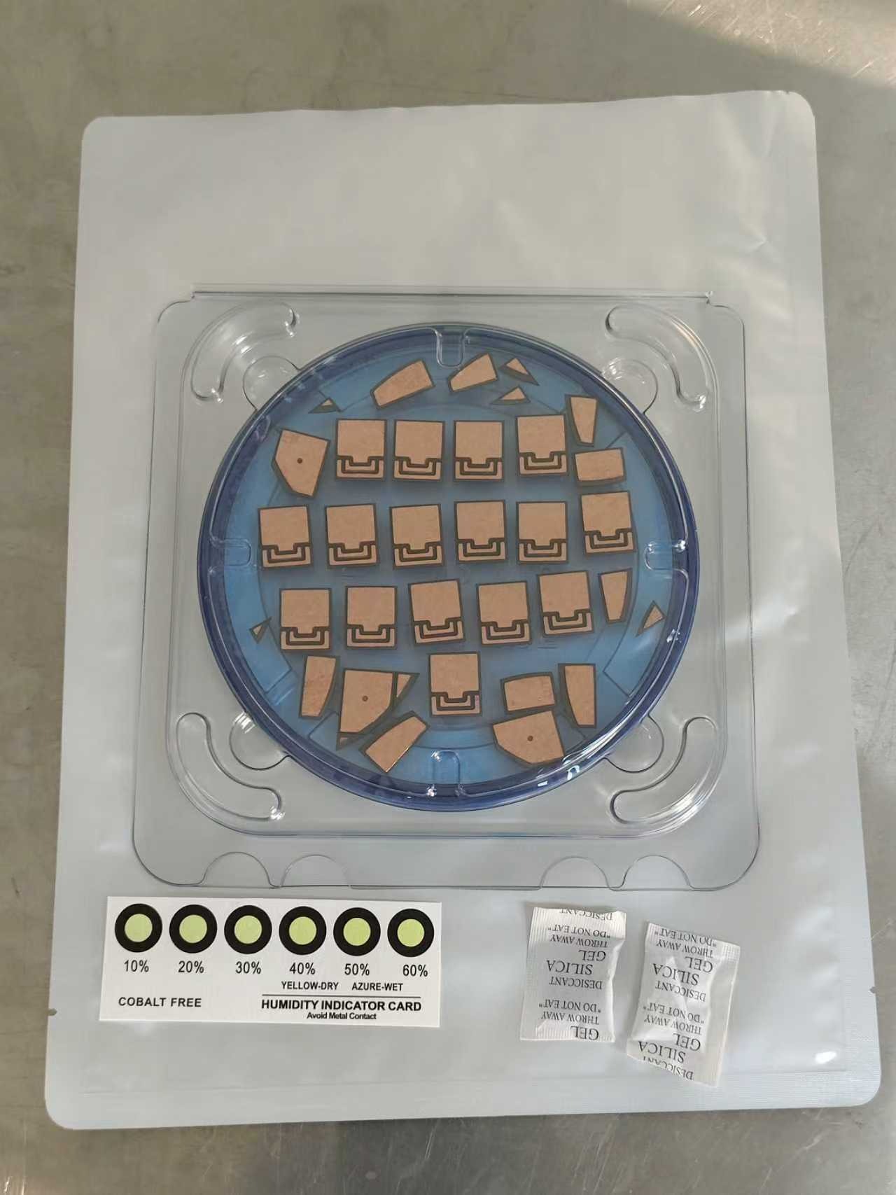
Baineng Yunban Diamond Substrate Product Image
Baineng Yunban Diamond Core Capabilities
1. Ultra-High Thermal Conductivity Breaks Thermal Bottlenecks
Diamond substrate achieves thermal conductivity of 1800–2200 W/(m·K), which is 4–5 times that of conventional AlN substrates and 3–4 times that of Si₃N₄ substrates, enabling ultra-fast heat dissipation pathways. Combined with an 800 μm double-sided thick copper structure, thermal spreading efficiency increases by over 50%, effectively stabilizing the junction temperature of SiC/GaN devices and eliminating thermal accumulation risks at the source.
2. Mature AMB Process Ensures Maximum Reliability
Baineng Yunban has deep expertise in AMB technology, achieving atomic-level metallurgical bonding between diamond and thick copper layers, with interfacial bond strength exceeding 30 MPa—far surpassing industry standards. The substrate withstands extreme thermal cycling from -40°C to 150°C without delamination, cracking, or void formation, making it ideal for demanding applications such as automotive and rail transportation.
3. Customized Precision Manufacturing for Diverse Applications
Supports standard Φ100 mm base wafers with flexible panel layouts (approx. 18 units per panel). High-precision etching and dicing maintain tolerances within ±20 μm. Customization options include copper thickness, pattern layout, and surface finish, perfectly matching various packaging and power requirements to enable miniaturization and high integration.
4. End-to-End Quality Control for Consistent Delivery
A comprehensive quality control system covers every stage from raw material to finished product, rigorously inspecting appearance, blisters, porosity, and void content to ensure consistency. Adhering to a “non-destructive testing” principle, only fully qualified products are shipped, while also supporting customer-led reliability validation to accelerate project implementation.
Baineng Yunban Benchmark Case Study | Industrial High-Power Servo Drive
Industry Pain Point: The Core Conflict Between Size Reduction and Thermal Performance Blocks Entry into Premium Markets
A leading Chinese industrial automation company targeting high-end CNC machine tools faced stringent upgrade requirements for its high-power servo drives: power module volume must be reduced by 30% without compromising thermal performance, while maintaining stable operation under 1.5x overload conditions. Traditional ceramic substrate solutions failed entirely—reducing size drastically cut heat dissipation area, causing junction temperatures to exceed limits, resulting in sluggish response, reduced positioning accuracy, and failure to pass long-term industrial reliability tests, thus blocking access to premium markets.
Baineng Yunban Solution: Diamond AMB Thick Copper Substrate Delivers Breakthrough Performance
Addressing the client’s core challenges, Baineng Yunban leveraged its proprietary technology to deliver a customized thermal solution: selecting high-thermal-conductivity diamond substrate and combining it with in-house AMB process to create an 800 μm double-sided thick copper structure. Through optimized panel layout and precision etching/dicing, the solution achieved a 30% volume reduction while maximizing thermal efficiency—perfectly balancing miniaturization and high-performance cooling.
Tangible Results: Data Validates Baineng’s Leadership and Opens Premium Markets
Size Target Achieved: Power module volume precisely reduced by 30%, enabling compact equipment design
Thermal Performance Enhanced: Module thermal spreading efficiency increased by 50%; junction temperature remained within spec even under 1.5x overload
Performance Doubled: Equipment response speed improved by 20%, with industry-leading positioning accuracy and stability
Market Breakthrough: Enabled client to successfully enter the high-end machine tool market, significantly boosting market share
Customer Testimonial: “Baineng Yunban’s diamond substrate solved our most critical challenge with cutting-edge technology. Both product performance and service exceeded expectations—it’s our key partner for premium market expansion!”
Additional Industry Success Stories
Case 2: 1500V Photovoltaic Energy Storage Inverter
Pain Point: Outdoor high temperatures and frequent charge/discharge cycles overwhelmed traditional Si₃N₄ substrates, reducing efficiency and lifespan
Results: Thermal resistance reduced by 42%; conversion efficiency reached 99.2%; operated fault-free for 1000 hours at 125°C; O&M costs reduced by 28%
Case 3: Rail Transit Traction Inverter
Pain Point: Limited space required higher power density, but wide-temperature reliability fell short
Results: Module volume reduced by 25%; power density increased by 40%; passed EN 50155 rail standard; deployed in 350 km/h high-speed rail systems
Typical Application Scenarios
New Energy Vehicles: Core power modules including motor controllers, OBC, DC-DC converters, and onboard chargers
Rail Transportation: High-voltage, high-power components such as traction inverters, auxiliary power supplies, and signal control units
Industrial Control: High-power inverters, servo drives, PV inverters, and industrial power supplies
Aerospace: High-reliability power electronics and satellite power modules for extreme environments
Power & Energy: High-power electronic equipment including smart grids, energy storage inverters, and HVDC transmission systems
Baineng Yunban Service Commitments
Customization: Dedicated engineering team provides one-on-one support for tailored dimensions, copper thickness, and pattern designs
On-Time Delivery: Full cycle from prototyping to production takes approx. 2.5 months, supporting both small-batch trials and large-volume stable delivery
End-to-End Technical Support: Comprehensive services covering design simulation, process optimization, and reliability validation
Flexible Testing Options: Supports customer-led reliability testing with complete inspection reports for seamless project execution
Baineng Yunban empowers next-generation high-power devices with diamond-grade thermal performance!
trending news
Contact Us