



Sorry, no sales person is available right now to take your call. Pls leave a message and we will reply to you via email as soon as possible.
Home/ PCB News/ ENIG, Gold Plating, Nickel-Gold, Palladium-Gold, Thick Gold, Thin Gold, Immersion Gold: A Complete Guide to PCB Gold Finishes
ENIG, Gold Plating, Nickel-Gold, Palladium-Gold, Thick Gold, Thin Gold, Immersion Gold: A Complete Guide to PCB Gold Finishes
2026-03-17
Engineers working on hardware, RF, PCB prototyping, and micro-assembly are most easily confused by the various "gold processes":
ENIG, electroplated gold, nickel-gold, immersion gold, thick gold, thin gold, palladium-gold, immersion gold…
Names differ by just one or two characters, yet cost, reliability, high-frequency performance, solderability, and bondability vary drastically.
No fluff today—straight to the point by:
Common Name → Plating Structure → Process Flow → Pros/Cons → Applications → Restrictions → Cost
We’ll clarify all surface finishes once and for all—so you’ll never choose wrong again.
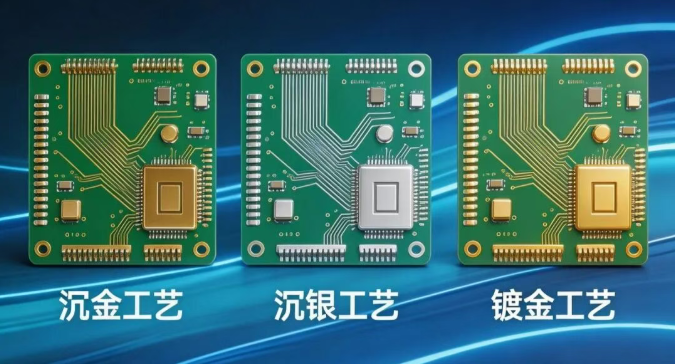
I. First, unify the concepts: All gold processes fall into two main categories
1. Chemical Gold (ENIG / Immersion Gold): No electricity—relies on chemical reaction → ultra-flat, ideal for BGA.
2. Electroplated Gold: Requires electrical current → thick, wear-resistant, suitable for connectors/plug-in contacts and wire bonding.
All terms like “nickel-gold,” “palladium-gold,” “thick gold,” and “thin gold” are subtypes of these two categories.
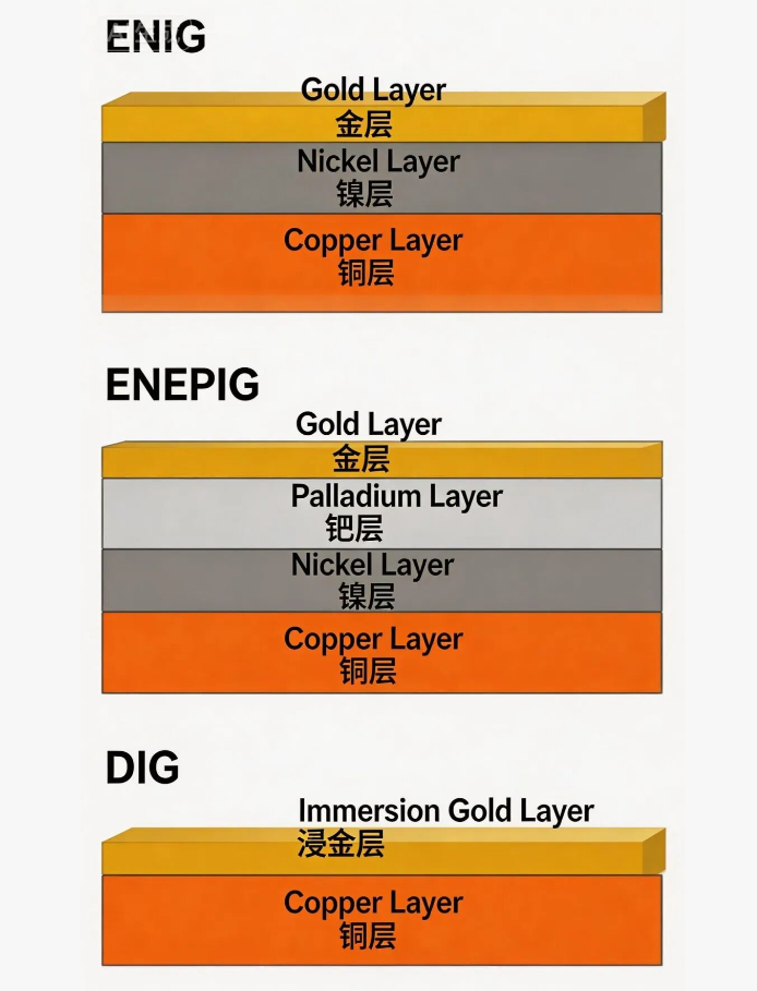
II. ENIG (Electroless Nickel Immersion Gold) = Chemical Nickel-Gold (Most Common)
Full name: Electroless Nickel Immersion Gold.
Chinese term: Electroless nickel plating + immersion gold plating.
Industry nicknames: ENIG, immersion gold, nickel-gold.
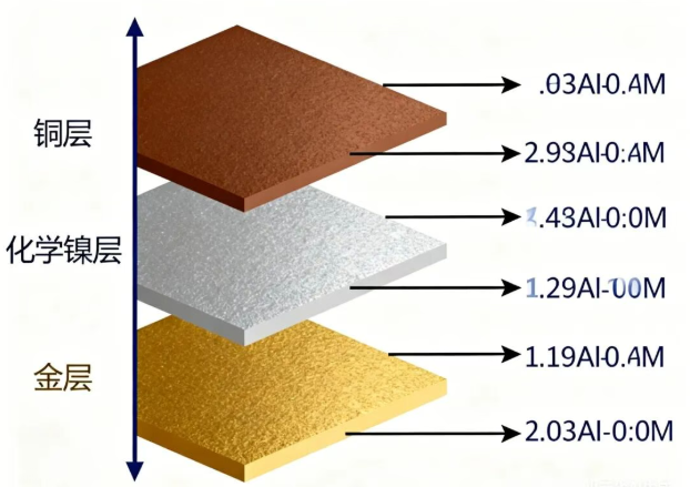
1. Structure (Critical!)
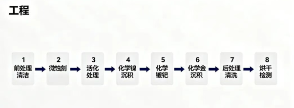
Copper → Electroless nickel layer (3–5 μm) → Gold layer (0.05–0.1 μm).
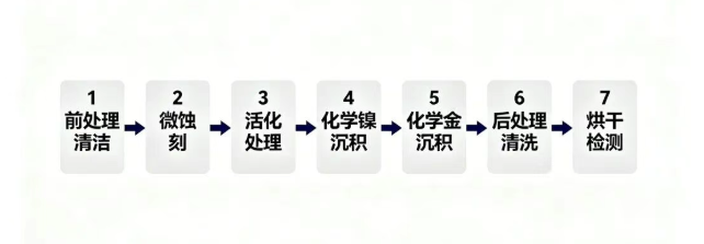
2. Process Flow
Key Characteristics
Extremely flat—perfect for BGA/QFN/fine-pitch ICs.
Stable soldering, minimal risk of cold joints.
Long shelf life.
Moderate cost—preferred for mass production.
Critical Drawback (Must-Know for RF Engineers)
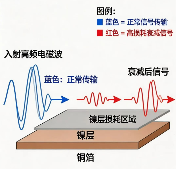
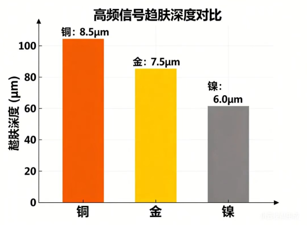
Contains nickel! Nickel is ferromagnetic (μr ≈ 100–600) and has only ~1/4 the conductivity of copper.
Due to skin effect at high frequencies, signals penetrate the thin gold layer and enter the nickel layer, causing:
Hysteresis loss + eddy current loss.
Losses explode as frequency increases.
Measured insertion loss comparison (microstrip line):
1 GHz: Nickel-containing processes show 40%–80% higher loss than bare copper or immersion silver
10 GHz: Loss increases by 100%–200%
28/77 GHz mmWave: Loss increases by 3–5×
Directly impacts sensitivity and transmission range.
Root Cause
Nickel’s extremely high magnetic permeability results in very shallow skin depth, drastically reducing effective conductive area.
Nickel’s conductivity is only 1/4 that of copper, leading to sharply increased conductor loss.
Hysteresis + eddy current losses scale with the square of frequency, deteriorating rapidly at high frequencies.
Applications / Restrictions
Recommended for: Consumer electronics, BGA, high-volume production.
Avoid for: RF / high-frequency / mmWave circuits, edge connectors (gold fingers), frequent plugging/unplugging.
ENEPIG = Nickel + Palladium + Gold (Premium ENIG)
Full name: Electroless Nickel Electroless Palladium Immersion Gold
Nicknames: Palladium-gold, ENEPIG, "black pad-free" ENIG.
Structure
Copper → Electroless nickel → Palladium layer (0.05–0.1 μm) → Gold layer.
Key Characteristics
Adds a palladium layer over ENIG to completely eliminate black pad issues.
Exceptional reliability—ideal for mission-critical applications.
30%–50% more expensive than standard ENIG.
High-Frequency Performance
Still contains nickel → high-frequency losses remain severe. Not recommended for RF boards.
(Improved reliability, but RF performance is nearly identical to ENIG—no fundamental improvement)
Applications / Restrictions
Recommended for: Automotive, medical, military, high-reliability products.
Avoid for: RF / high-frequency PCBs.
Electroplated Gold = Thick Gold, Thin Gold, Hard Gold, Soft Gold
Nicknames: Plated gold, electroplated gold.
Structure (99.9% of industry cases)
Copper → Electroplated nickel (5–8 μm) → Electroplated gold (0.1–3 μm).
Key Takeaway
Standard PCB electroplated gold ALWAYS contains nickel!
Nickel acts as an adhesion layer, stress buffer, and diffusion barrier—it cannot be omitted.
Nickel-free "pure gold" processes are not called electroplated gold—they are known asDirect Immersion Gold (DIG).
Thick Gold vs. Thin Gold
Thin Gold (0.1–0.3 μm)
Lower cost—suitable for test points and simple edge connectors.
Thick Gold (0.5–3 μm)
Ideal for wire bonding, high-frequency connectors, and military applications.
Hard Gold vs. Soft Gold
Hard Gold (cobalt/nickel alloy): Wear-resistant → edge connectors, plug-in contacts, connectors.
Soft Gold (pure gold): Bonding-specific → IC pads, gold ball bonding.
Why Electroplated Gold Is Unsuitable for RF?
It’s not the gold—it’s the nickel!
As long as nickel is present, it introduces massive high-frequency losses.
Even thin electroplated gold can’t avoid this—because the nickel layer remains.
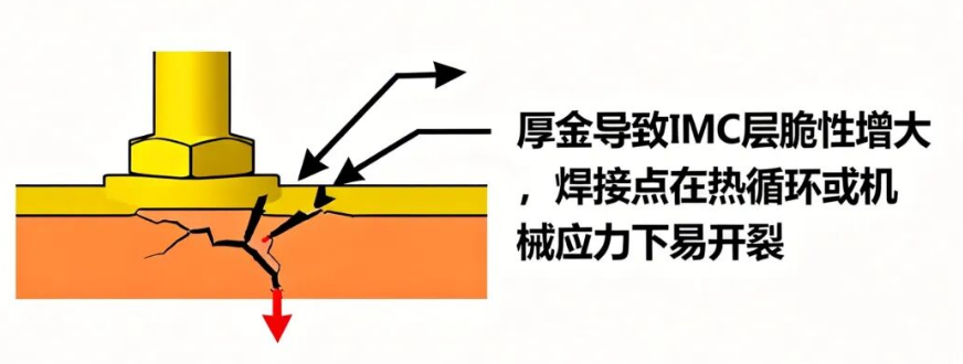
Why Thick Electroplated Gold Is Bad for SMT Soldering?
Poor wettability—solder "doesn’t wet" gold well.
Forms brittle Au-Sn intermetallic compounds (IMCs), leading to cracked joints.
Poor planarity—prone to BGA voiding.
Remember: Thick gold is ONLY for bonding—not for soldering!
Correct Usage for RF Micro-Assembly Boards
Bonding Pads: Local thick electroplated gold (≥0.5 μm)
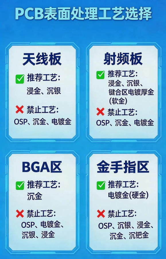
RF Traces: Absolutely NO gold plating—use OSP / immersion silver / DIG instead.
If full-board gold is mandatory: use ultra-thin gold (0.05–0.1 μm) so signals travel through copper via skin effect.
DIG (Direct Immersion Gold) = Nickel-Free Pure Gold (RF-Specific)
Full name: Direct Immersion Gold
Nicknames: Direct immersion gold, nickel-free gold, pure gold finish.
Structure
Copper → Gold
Features
Completely nickel-free → optimal for RF / mmWave performance.
High planarity.
Ultra-thin gold layer (0.02–0.05 μm).
Not suitable for wire bonding, plugging, or thickening.
Applications / Restrictions
Recommended for: RF, microwave, mmWave, high-frequency transmission lines.
Avoid for: Wire bonding, plugging, high-reliability scenarios.
Other Mainstream Surface Finishes
OSP (Organic Solderability Preservative)
Copper + transparent organic film—nickel-free, cheapest, excellent for RF, but scratch-sensitive.
Recommended for: RF boards, low-cost boards, BGA.
Hot Air Leveling (HASL)
Copper + tin layer—inexpensive, good solderability, but poor planarity.
Avoid for: BGA, RF boards.
Immersion Silver
Nickel-free, excellent for RF/high-speed, but prone to tarnishing.
Recommended for: RF, high-frequency, high-speed PCBs.
Immersion Tin
Nickel-free, flat, good solderability, short shelf life.
Recommended for: Cost-effective high-frequency boards.
| Process Name | Common Name | Structure | Contains Nickel? | Planarity | Solderability | Bondability | RF/High-Freq Performance | Primary Use | Restrictions |
|---|---|---|---|---|---|---|---|---|---|
| ENIG | ENIG | Nickel-Gold, Immersion Gold | Cu → Ni → Au | Yes | Excellent | Excellent | No | Poor (3–5× higher loss) | BGA, consumer electronics |
| ENEPIG | ENEPIG | Palladium-Gold | Cu → Ni → Pd → Au | Yes | Excellent | Excellent | No | Poor (same as ENIG) | Automotive, medical, military |
| Electroplated Gold | Plated Gold | Cu → Ni → Au | Yes | Fair | Poor | Yes | Poor | Bonding, edge connectors | Full-board use, BGA |
| Thick Electroplated Gold | Thick Gold | Cu → Ni → Thick Au | Yes | Fair | Very Poor | Excellent | Poor | Wire bonding | RF traces, soldering |
| Thin Electroplated Gold | Thin Gold | Cu → Ni → Thin Au | Yes | Fair | Poor | Fair | Poor | Test points, simple edge connectors | RF traces |
| DIG | DIG | Nickel-Free Gold | Cu → Au | No | Good | No | Yes | Excellent (near bare copper) | RF, mmWave |
| OSP | Anti-Oxidation | Cu → Organic Film | No | Excellent | Good | No | Excellent | RF, low-cost | Contact, plugging |
| Immersion Silver | Immersion Silver | Cu → Ag | No | Good | Good | No | Excellent | RF, high-frequency | Harsh environments |
| HASL | Hot Air Leveling | Cu → Sn | No | Poor | Good | No | Poor | Power supplies, through-hole boards | BGA, high-frequency |
| Immersion Tin | Immersion Tin | Cu → Sn | No | Good | Good | No | Very Good | Cost-effective high-frequency | High-reliability |
Key Takeaways (Engineers—Memorize This)
Nickel-Gold = ENIG—both contain nickel and are unsuitable for RF.
Palladium-Gold = ENEPIG—more reliable but still contains nickel and is unsuitable for RF.
Plated Gold = Electroplated Gold—always contains nickel, causing high RF losses.
Thick gold is for bonding; thin gold is for contact points—neither should be used on RF traces.
Only DIG is a nickel-free pure gold process—best RF performance, but not bondable.
Standard RF Micro-Assembly Approach:
Transmission lines → DIG / immersion silver / OSP
Bonding pads → Local thick electroplated gold
Plated Gold ≠ DIG
Plated Gold: Contains nickel, can be thickened, bondable
DIG: Nickel-free, very thin, RF-specific
Nickel is devastating for high frequencies:
Insertion loss doubles at 10 GHz; increases 3–5× in mmWave,
due to: high permeability + low conductivity.
trending news
Contact Us