



Sorry, no sales person is available right now to take your call. Pls leave a message and we will reply to you via email as soon as possible.
Home/ PCB News/ A Comprehensive Analysis of the Entire Manufacturing Process for Low-Temperature Co-fired Ceramic (LTCC) Substrates
A Comprehensive Analysis of the Entire Manufacturing Process for Low-Temperature Co-fired Ceramic (LTCC) Substrates
2026-09-20
Low Temperature Co-fired Ceramic (LTCC) technology holds a significant position in the field of electronic packaging due to its excellent high-frequency characteristics, high integration density, and fine wiring capabilities. LTCC substrates are widely used in microwave and millimeter-wave high-frequency modules, sensor packaging, Multi-Chip Modules (MCM), MEMS packaging, semiconductor interposer substrates, T/R components, and Co-Packaged Optics (CPO).
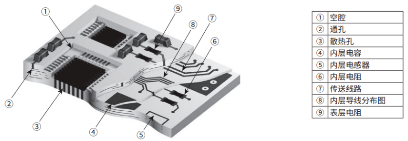
Figure 1: Structure Diagram of an LTCC Substrate
The manufacturing process of LTCC substrates primarily includes slurry preparation, tape casting, punching, hole drilling, via filling, pattern printing, lamination, isostatic pressing, cutting, binder burnout and co-firing, post-printing, post-firing, nickel/gold plating, resistance trimming, and inspection. The following sections provide a brief analysis of each step.
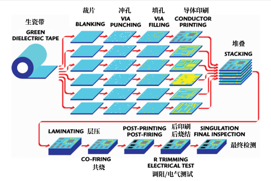
Figure 2: Manufacturing Process Flow of LTCC Substrates
1. Slurry Preparation
Ceramic powders, glass powders, and organic carriers are mixed according to a specific formulation ratio. Through ball milling, dispersion, and degassing treatments, a slurry with uniform composition and stable performance is produced. Organic carriers typically include solvents, binders, plasticizers, and dispersants, whose ratios directly affect the forming quality and sintering performance of the green ceramic tape.
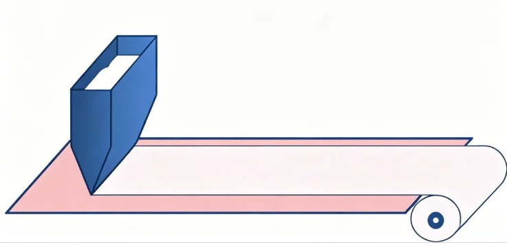
2. Tape Casting
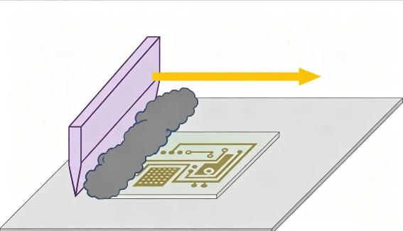
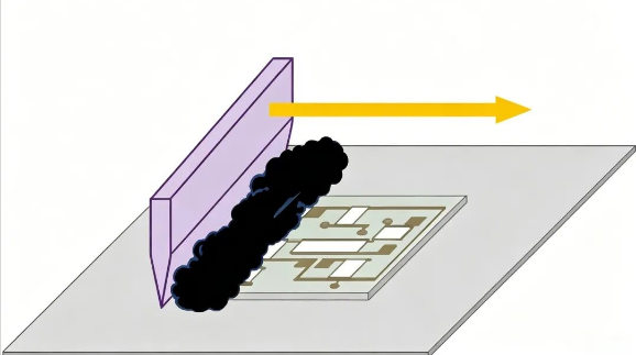
After degassing and defoaming, the slurry is uniformly coated onto a carrier film using a tape casting machine, then dried and cured to form dense green ceramic tapes with uniform thickness and certain mechanical strength. The tape casting process requires strict control of parameters such as slurry viscosity, doctor blade gap, and drying rate to ensure consistent tape thickness and surface quality.
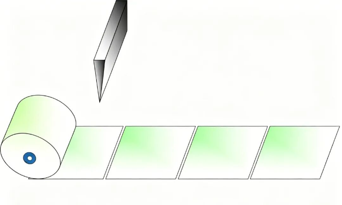
3. Punching/Cutting
Rolled green ceramic tapes are cut according to design dimensions. Cutting sizes are usually slightly larger than final product dimensions to reserve processing margins for subsequent steps such as hole drilling, printing, lamination, and cutting.
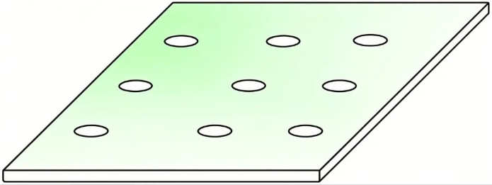
4. Hole Drilling
Vias, through-holes required for electrical interconnection, and alignment holes are created on the green ceramic sheets using mechanical or laser drilling methods. Hole position accuracy, diameter consistency, and wall quality directly affect subsequent via filling results and interlayer connection reliability.
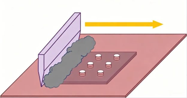
5. Via Filling
Conductive paste is filled into vias through micro-via injection or screen printing processes to form vertical pathways connecting circuits between layers. Via filling must ensure dense filling without voids and maintain good connectivity with subsequently printed patterns.
6. Pattern Printing
Screen printing technology is used to print conductive pastes or dielectric materials onto green ceramic sheets to create electrical interconnection traces, pads, and embedded components such as resistors, capacitors, and varistors. This step requires control over line width, line spacing, film thickness, and registration accuracy.
7. Lamination
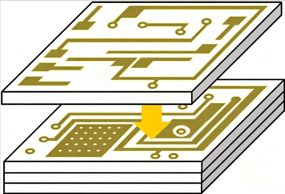
Green ceramic sheets with printed circuit patterns are stacked sequentially according to the pre-designed number of layers and order. Lamination molds typically feature alignment pins consistent with the alignment holes on the green sheets, or optical alignment systems are used to ensure precise layer-to-layer alignment.
8. Isostatic Pressing
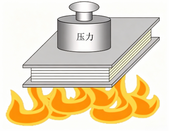
Isostatic pressing is employed under specific temperature and pressure conditions to tightly bond multiple layers of green ceramic sheets into a complete multi-layer substrate body. This step is typically Warm Isostatic Pressing (WIP), which helps improve interlayer bonding strength and reduce defects such as delamination and voids.
9. Cutting
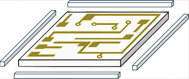
Large-area green ceramic bodies are cut and separated along the boundaries of individual modules to facilitate subsequent sintering. Cutting methods may include mechanical cutting, hot wire cutting, etc., requiring neat edges and accurate dimensions.
10. Binder Burnout and Co-firing
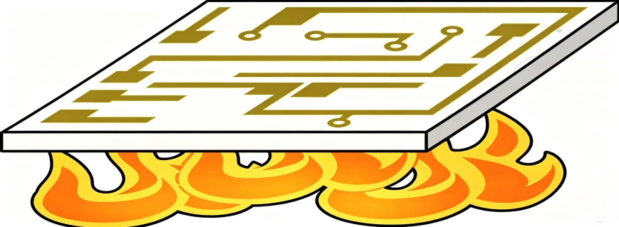
The cut green ceramic bodies are placed on setter plates inside a sintering furnace and undergo binder burnout and co-firing according to a set temperature profile. The binder burnout stage removes organic components, while the sintering stage densifies the ceramic and conductor together, ultimately yielding a dense LTCC fired ceramic substrate. LTCC co-firing temperatures are typically around 850–900°C, requiring strict control of atmosphere, heating rate, and shrinkage matching.
11. Post-Printing
Thick-film conductor layers or resistor pastes are printed onto the surface of the sintered LTCC substrate to form surface interconnections, pads, and thick-film resistors. Post-printing can utilize different paste systems and patterns based on product design requirements.
12. Post-Firing
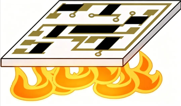
The substrate after post-printing is fired according to thick-film paste process requirements, typically in an air atmosphere, to ensure good bonding between surface thick-film resistors or conductor layers and the LTCC substrate, achieving target electrical properties.
13. Nickel/Gold Plating
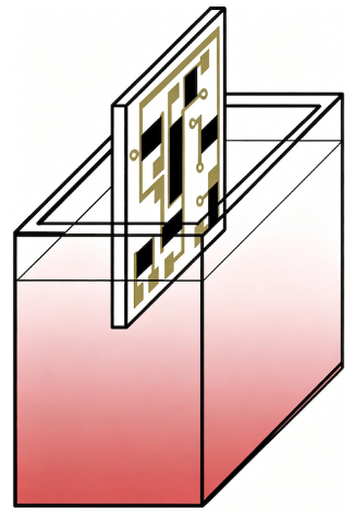
Electroless nickel/gold plating processes are used to form nickel and gold layers on conductor areas of the substrate surface, enhancing solderability, wire bondability, and oxidation resistance. Common techniques include Electroless Nickel Immersion Gold (ENIG), requiring control over plating thickness and uniformity.
14. Resistance Trimming
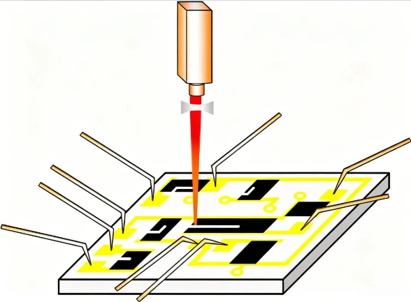
Laser trimming technology is used to adjust resistors on the LTCC substrate surface by cutting the resistor body to change its value until it reaches the target resistance. Laser trimming offers advantages such as high precision, non-contact operation, and real-time monitoring.
15. Inspection
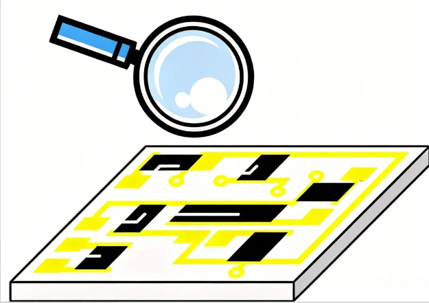
Finished LTCC substrates undergo inspection covering items such as warpage, dimensional accuracy, cosmetic defects, electrical performance, solderability, bond strength, and reliability to ensure products meet design and usage requirements.
In summary, LTCC substrate manufacturing is a precise process involving the coordination of multiple steps. These steps are interconnected, requiring key control over parameters such as slurry homogeneity, green tape thickness, hole position accuracy, via filling quality, printing registration, lamination uniformity, shrinkage matching, and sintering profiles to ensure the final substrate possesses excellent dimensional accuracy, electrical performance, and long-term reliability.
trending news
Contact Us