



Sorry, no sales person is available right now to take your call. Pls leave a message and we will reply to you via email as soon as possible.
Home/ PCB News/ A Comprehensive Guide to Selecting Ceramic Substrates for High-Speed Optical Modules: Thermal Mechanisms, Processes, Applications, and Pitfalls to Avoid for Alumina vs. Aluminum Nitride
A Comprehensive Guide to Selecting Ceramic Substrates for High-Speed Optical Modules: Thermal Mechanisms, Processes, Applications, and Pitfalls to Avoid for Alumina vs. Aluminum Nitride
2026-09-08
This article systematically compares and analyzes the application selection of alumina (Al₂O₃) and aluminum nitride (AlN) ceramic substrates in high-speed optical modules from multiple dimensions, including thermal conduction physics, thermal management engineering measurements, CTE matching, hydrolysis reliability, processing technology, metallization routes, cost structure, and industry trends. Based on widely accepted industry test data and engineering experience, this paper aims to provide actionable technical references for thermal design, packaging processes, and supply chain decisions in optical modules. Key conclusion: Neither material is universally superior; their suitability depends on specific application scenarios, leading to a stratified coexistence in the industry.
I. Industry Background: Thermal Management Defines the Reliability Ceiling of Optical Modules
Approximately 55% of electronic component failures are directly or indirectly caused by temperature. Industry experience shows that for every 2°C increase in ambient temperature, overall device reliability drops by about 10%. As optical modules evolve toward higher speeds and greater density, power consumption grows exponentially. The typical power consumption ranges for mainstream products are as follows:
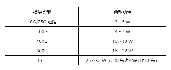
An even more stringent constraint comes from package size: mainstream form factors such as QSFP-DD and OSFP are strictly defined by MSA protocols. Module power consumption has increased nearly sixfold compared to earlier generations, while the external surface area available for heat dissipation remains largely unchanged. This means heat cannot be dissipated by expanding physical space but must travel along the fixed path: chip → bonding layer → ceramic substrate → heatsink → air.
In this thermal path, the ceramic substrate serves four critical functions: electrical routing, electrical insulation, heat transport, and mechanical support. Its material properties directly determine the thermal management ceiling and long-term reliability of the module.
Optical devices face an additional hidden constraint: the wavelength temperature drift coefficient of DFB lasers is approximately 0.1 nm/°C. Higher substrate thermal resistance leads to higher chip junction temperatures, which increases the cooling load and power consumption of the TEC (thermoelectric cooler), further raising temperature and creating a vicious cycle: ↑ temperature rise → ↑ wavelength drift → ↑ TEC power → ↑ further temperature rise.
Therefore, ceramic substrate selection is fundamentally about the systematic allocation of the module’s thermal budget, stress budget, and high-frequency loss budget—not merely a simple material substitution.
Key Selection Conclusion (Stratified Coexistence, Not Replacement)
Low-cost, medium-to-low speed, hermetic packaging scenarios → Prefer alumina (Al₂O₃) for optimal cost-performance ratio.
High heat flux density, CTE matching required for InP/Si/GaAs chips, 50G+ high-speed/high-frequency, high-reliability scenarios → Prefer aluminum nitride (AlN) for performance assurance.
II. Thermal Conduction Mechanism: The Physical Origin of the 7× Thermal Conductivity Gap
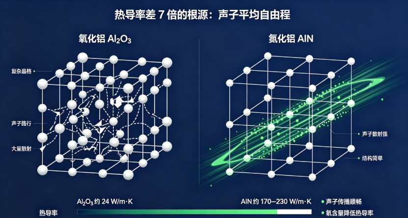
Ceramic materials lack free electrons; thus, heat conduction primarily relies on phonons (quanta of lattice vibrations). The lower the phonon scattering and the longer the mean free path, the higher the thermal conductivity. The inherent differences in crystal structure between the two materials create a natural performance gap.
Alumina (Al₂O₃): Inherently Limited Thermal Conductivity
Alumina features a mixed ionic-covalent crystal lattice with complex structure, heavy oxygen atoms, and strong lattice anharmonicity, resulting in severe phonon scattering that significantly limits thermal efficiency. Its intrinsic thermal conductivity ceiling is approximately 30 W/m·K, and the typical value for commercial 96%-purity substrates is only 24 W/m·K—a physical limit that cannot be overcome by formulation or conventional processing.
Aluminum Nitride (AlN): Natural Structural Advantage for High Thermal Conductivity
AlN has a simple wurtzite crystal lattice with strong covalent bonds and light constituent atoms (Al: 27, N: 14), resulting in highly ordered lattice vibrations and a much longer phonon mean free path than alumina. The theoretical thermal conductivity of single-crystal AlN can reach 320 W/m·K. Commercial polycrystalline products consistently achieve 170–230 W/m·K, with high-purity premium grades exceeding 230 W/m·K—making AlN’s overall thermal performance 6–8 times that of alumina.
AlN’s Key Weakness: Catastrophic Degradation from Oxygen Contamination
The actual thermal conductivity of AlN is almost entirely determined by its oxygen content, a well-known industry pain point. When oxygen atoms enter the lattice, they substitute nitrogen sites and simultaneously create aluminum vacancies to maintain charge neutrality. These lattice defects strongly scatter phonons, causing thermal conductivity to plummet dramatically. Supporting data shows: when oxygen content rises from 0.5 wt% to 2 wt%, thermal conductivity can drop from 200 W/m·K to below 100 W/m·K.
This triggers a chain reaction: powder moisture absorption → hydrolysis → oxygen impurity introduction → increased lattice defects → intensified phonon scattering → severe thermal conductivity degradation. This explains why the entire AlN supply chain must rigorously control humidity, exclude moisture, and use inert atmospheres during production—a key to understanding its process complexity.
III. Comprehensive Parameter Comparison
The table below presents parameters for mainstream commercial specifications (compiled from manufacturer datasheets and third-party test data). For actual selection, batch-specific test reports must be used—never rely solely on nominal values:
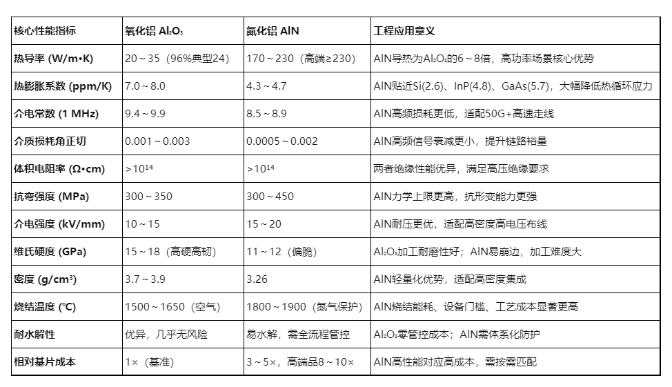
In terms of material coverage, domestic manufacturers now offer mass production capabilities for alumina, aluminum nitride, and silicon nitride ceramic substrates. For example, BaiNeng YunBan provides ceramic substrate processing for 1–6 layer high-precision ceramic PCBs, with thicknesses ranging from 0.20–1.5 mm and minimum line/space down to 0.075 mm / 0.040 mm, offering viable engineering options for high-density optical modules.
IV. Thermal Performance: From 1D Thermal Resistance to 3D Spreading Resistance – Engineering Measurements
Common industry misconception: focusing only on 1D vertical thermal resistance while ignoring the core challenge in optical modules—3D spreading thermal resistance. Using the 1D steady-state conduction formula R = L / (k × A), we quantify the difference:
Case A: Overall Vertical Conduction (Uniform Heat Source)
Conditions: Chip mounting area 10×10 mm (A = 1×10⁻⁴ m²), substrate thickness 0.5 mm (L = 5×10⁻⁴ m), heat flow 10 W
Alumina (k=24): R = 0.208 K/W, ΔT = 2.08 °C
AlN (k=170): R = 0.029 K/W, ΔT = 0.29 °C
Under 1D conditions, the temperature difference is only 1.8 °C—seemingly minor. However, this assumes an idealized uniform heat source, which does not reflect real-world optical modules.
Case B: Real-World Conditions – Hotspot 3D Spreading Resistance (The Critical Battlefield)
DSPs and laser drivers (LDDs) in optical modules are not uniform heat sources but rather millimeter/sub-millimeter-scale hotspots with local heat flux densities exceeding 50 W/cm². Heat spreads three-dimensionally from these tiny hotspots across the entire substrate, making lateral heat-spreading capability the primary bottleneck—not vertical conduction.
Spreading resistance is highly sensitive to material thermal conductivity. AlN’s 6–8× advantage is fully leveraged here, resulting in hotspot temperature reductions far exceeding 1.8 °C. Engineering experience provides clear thresholds:
Module total power > 20 W
Local hotspot heat flux density > 50 W/cm²
Below these thresholds, alumina is fully adequate; above them, AlN becomes essential for reliability.
Critical Pitfall Warning
When interfacial thermal resistance (solder voids, TIM layers, bonding interface defects) dominates total thermal resistance, simply replacing Al₂O₃ with AlN yields diminishing returns—often resulting in “5× cost increase for <10% performance gain”.
Optimization priority: First improve interfacial processes (reduce voids, optimize TIM thickness/material, eliminate defects), then upgrade substrate material.
Additionally, AlN’s thermal conductivity degrades at elevated temperatures. Selection must be based on actual operating temperatures (60–85 °C)—never use room-temperature (25 °C) nominal values.
V. CTE Matching: The Invisible Pillar of Optical Device Reliability
Thermal expansion coefficient (CTE) mismatch induces cyclic thermal stress, a primary cause of solder joint fatigue, chip cracking, metal plating delamination, and bond failure. Optical communication devices are far more sensitive to CTE matching than standard power devices. Key material CTE values (ppm/K):
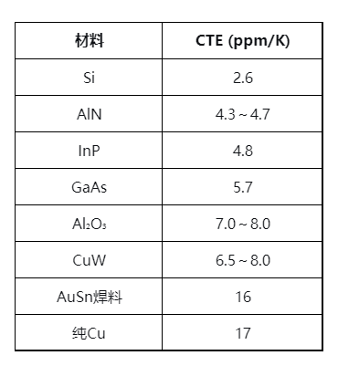
High-speed optical modules commonly use InP-based EML lasers (CTE ≈ 4.8) and AuSn solder (CTE ≈ 16), which are inherently mismatched and prone to shear stress during thermal cycling.
AlN’s CTE (4.3–4.7) closely matches InP, Si, and GaAs photonic chips, acting as a stress-buffering transition layer. This significantly reduces shear deformation in solder joints during temperature cycling (-40 to 85 °C), effectively suppressing void growth and crack initiation after 500–1000 cycles, offering substantially better long-term reliability than alumina.
Secondary Benefits: Improved substrate temperature uniformity reduces laser junction temperature variation and wavelength drift (mitigating the 0.1 nm/°C risk). Simultaneously, TEC cooling load decreases, creating a “stable temperature → lower power → reduced heating” positive feedback loop. For CWDM/LWDM systems with tight channel spacing, this performance is a mandatory requirement—not a luxury.
VI. Hydrolysis: AlN’s Fatal Flaw and Systematic Mitigation Strategies
Hydrolysis is AlN’s most critical weakness compared to alumina and the most underestimated reliability risk. Alumina, as a stable oxide, has no hydrolysis risk; AlN, as a metastable nitride, undergoes irreversible reaction with water:
The resulting aluminum hydroxide (which converts to boehmite) and ammonia gas degrade the product in three ways:
Raw Powder: High-surface-area AlN powder forms an insulating aluminum hydroxide layer in humid environments. During high-temperature sintering, this hydrolyzed layer decomposes and releases oxygen impurities, causing a catastrophic drop in final product thermal conductivity.
Processing: Wet processes like tape casting, grinding, dicing, cleaning, and plating all carry hydrolysis risks. Alkaline environments accelerate the reaction; acidic ones corrode surfaces, leading to whitening, powdering, and subsequent poor plating adhesion, blistering, and delamination.
Finished Product Reliability: Surface hydrolysis degrades solderability and wire bond strength; released ammonia corrodes adjacent metals and optical surfaces. Under harsh tests like 85°C/85%RH aging, PCT, and HAST, unprotected AlN substrates show significant performance degradation.
Six Core Process Solutions for AlN Hydrolysis Control
Powder Surface Modification: Hydrophobic coatings using phosphates, silane coupling agents, or stearic acid to block hydrolysis at the source.
Inert Dry Storage & Transport: Vacuum/nitrogen-sealed packaging with desiccants and humidity indicators; climate-controlled warehouses; strict time limits after opening.
Thermal Oxidation Passivation: Controlled oxidation at 1100–1300°C forms a dense 10–100 nm Al₂O₃ protective layer, providing hydrolysis resistance, improved surface energy, and compatibility with DBC transition layers.
Precision Wet Processing: Strict control of pH and duration in plating, cleaning, and dicing coolant; rapid drying between steps; prohibition of alkaline cleaners.
Pre-Use Activation: High-temperature baking for moisture removal, combined with plasma cleaning or mild acid etching to remove weak hydrolyzed layers and restore surface activity.
Reliability Validation Loop: Full coverage of 85°C/85%RH 1000h aging, PCT, and HAST testing; comparison of plating adhesion before and after reflow to eliminate process侥幸.
Objective Assessment: AlN hydrolysis is not unavoidable but requires systematic process control. Mature supply chains can support AlN passing automotive and telecom-grade reliability tests; uncontrolled adoption by incapable suppliers risks mass field failures. Alumina requires no extra controls, offering zero hidden costs—a key advantage in cost-sensitive applications.
Currently, only a few domestic suppliers possess full-process AlN control capabilities. For instance, BaiNeng YunBan has established a complete technical system covering material selection, ceramic substrate processing, multi-layer circuit design, metallization, and reliability validation. It meets automotive-grade quality standards for thermal shock, high-temperature aging, salt spray, vibration, and other rigorous tests, providing systematic assurance for reliability-critical applications like optical modules.
VII. Processing Technology: Similar Framework, Vastly Different Difficulty Levels
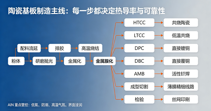
Alumina and aluminum nitride substrates share similar macro-level production steps (powder → tape casting → debinding → sintering → lapping → metallization → dicing → inspection), but differ drastically in equipment requirements, process windows, yield, and cost. The core difference can be summarized as: alumina is hard to “refine,” while AlN is hard to “make.”
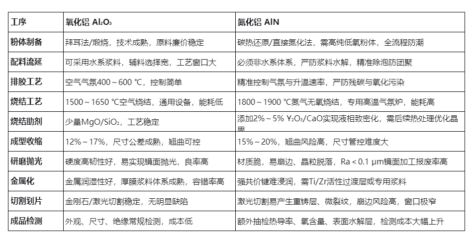
VIII. Seven Metallization Routes: Precision Matching for Optical Modules
Ceramic substrates require metallization for routing, die attachment, and heat conduction. Different routes determine line precision, current capacity, high-frequency performance, thermal efficiency, and cost. Selection guidelines for optical modules:
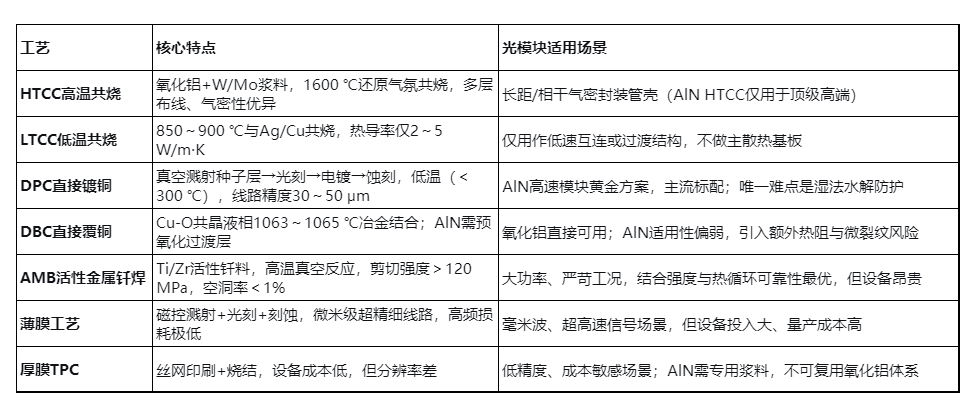
Notably, few manufacturers offer comprehensive capabilities in LTCC, HTCC, DBC, and DPC. BaiNeng YunBan achieves balance in thermal efficiency, line precision, environmental robustness, and integration density. Specifically:
LTCC process: Dielectric constant stable at 9.5 (1 MHz), loss tangent only 3×10⁻⁴, suitable for 5G mmWave (24–30 GHz) and microwave communications; embedding passive components reduces substrate volume by over 40%;
HTCC process: Density >98%, hermeticity ≤10⁻⁸ Pa·m³/s, CTE as low as 4.5×10⁻⁶/°C;
DBC process: Bond strength ≥25 MPa, current capacity up to 5 A/mm²;
DPC process: Electroplated copper tensile strength ≥200 MPa, resistance tolerance ≤±3%—meeting the core consistency requirements for high-speed signal routing in optical modules.
Quick Scenario Matching Guide
Chip Heat Spreaders / LD Submounts → AlN + DPC (preferred)
High-Power Hermetic Packages → Al₂O₃ + HTCC (cost-effective); high-end long-haul uses AlN HTCC/CuW
mmWave High-Frequency Routing → AlN + Thin Film/DPC
Cost-Sensitive Medium/Low-Speed Devices → Al₂O₃ + Thick Film
IX. Cost Analysis: Why It’s Expensive, Where the Gap Lies, and Paths to Cost Reduction
Price Multiplier: AlN substrates cost 3–5 times more than alumina of the same specification; high-thermal-conductivity (≥230 W/m·K) large-format products can reach 8–10 times. After DPC processing, the price gap stabilizes at 3–6 times.
AlN Core Cost Structure
High-Purity Powder (30–40%): Premium low-oxygen powder has long relied on imports, representing a key technological barrier.
High-Temperature Sintering (20–30%): Sintering at 1800°C+ in nitrogen atmosphere with long cycles incurs high equipment depreciation and energy costs.
Metallization (20–30%): Expensive vacuum sputtering equipment; high compliance and control costs for wet electroplating.
Processing & Inspection (10–20%): Precision polishing, chipping prevention, and specialized testing for thermal conductivity/oxygen content add significant premiums.
Alumina benefits from standardized mass-production costs with no extra premiums.
Four Key Cost-Reduction Pathways
Powder Localization: Domestic manufacturers have achieved breakthroughs in low-oxygen, high-purity AlN powder and high-thermal-conductivity substrates, breaking foreign monopolies.
Equipment & Process Upgrades: Continuous sintering furnaces replacing batch furnaces, large-format substrate production, and automated inspection boost capacity and yield.
Yield Ramp-Up: Each 1% yield improvement in AlN reduces costs far more significantly than in alumina, with strong economies of scale.
Vertical Integration: Integrated powder → substrate → metallization operations compress markup from intermediaries.
Hidden Cost Reminder: AlN has longer lead times, requires moisture-controlled inventory, and needs reliability validation upon introduction. Selection decisions should evaluate system-level total value—comparing AlN’s incremental cost against savings from reduced TEC power, improved wavelength stability, lower failure rates, and extended product life—not just substrate unit price.
From a supply chain perspective, vendors offering end-to-end integrated services—from material selection to finished delivery—can effectively reduce intermediary costs and accelerate product development cycles. BaiNeng YunBan’s scalable mass production of 1–6 layer high-precision ceramic PCBs, combined with flexible service models for prototypes, small/medium batches, and high-volume production, is specifically designed to meet this need.
X. Full-Scenario Selection Map and Quantitative Decision Thresholds
Scenario-Based Selection Guide
10G/25G Short-Reach, Low-Speed Devices → Al₂O₃ + Thick Film/DPC, optimal cost-performance
100G/400G Standard Modules → Primarily Al₂O₃, with localized AlN heat spreaders under DSP/LDD hotspots
800G Long-Haul, Coherent EML Devices → AlN Submount + AlN heat spreader/premium package
1.6T High-Density Silicon Photonics Modules → AlN as primary substrate (pilot production in 2026, volume ramp in 2027)
CPO Co-Packaged Optics → AlN nearly mandatory, as only it meets ultra-high heat flux and reliability demands
General Hermetic Packages → Al₂O₃ HTCC mainstream; high-end long-haul uses AlN HTCC/CuW
TEC Hot/Cold Side Substrates → High-power: AlN; low-power: Al₂O₃
50G+ High-Frequency/mmWave Applications → AlN + DPC/Thin Film for low-loss signal integrity
Automotive LiDAR, High-Power Laser Diodes → AlN + DPC, leveraging high thermal conductivity and reliability for harsh environments
In the high-end ceramic substrate segment, domestic manufacturers have already achieved stable mass production of AlN substrates with thermal conductivity >170 W/mK for AI optical modules, covering core applications in 5G/mmWave RF circuits, laser devices, and optical communication modules. Additionally, for specialized scenarios demanding extreme purity and optical performance, some suppliers offer high-performance single-crystal sapphire substrates (99.999% ultra-high-purity single-crystal α-Al₂O₃) as a differentiated option.
Quantitative Selection Thresholds
If any of the following is true, consider AlN:
Module total power > 20 W
Local hotspot heat flux density > 50 W/cm²
Precise CTE matching required for InP/Si/GaAs chips
Signal rates entering high-frequency/mmWave, loss-sensitive regimes
If any of the following is true, stick with alumina:
Cost-sensitive, medium/low power, short-reach general-purpose scenarios
Standard hermetic package required
Multiple wet processes or harsh humid environments, without AlN process control capability in the supply chain
XI. Top 10 Common Selection and Process Pitfalls
Blind Trust in Datasheets: Relying only on nominal thermal conductivity without requesting batch-specific laser flash test reports, ignoring batch variations and test condition discrepancies.
Ignoring Temperature Degradation: Using 25°C parameters without accounting for thermal conductivity decay at actual operating temperatures (60–85°C), leading to insufficient high-temperature cooling.
Poor Inventory Control: Using moisture-exposed AlN substrates without high-temperature baking, causing hydrolysis layers that lead to plating blistering, delamination, and bond failures.
Uncontrolled Wet Processes: Excessive plating/cleaning time or alkaline solutions catalyze hydrolysis, causing surface powdering and scrap.
Mixed Paste Usage: Applying alumina thick-film paste directly to AlN results in poor adhesion and inadequate long-term reliability.
Omitting Pre-Oxidation for AlN DBC: Non-oxide ceramics cannot be wetted by Cu-O eutectic liquid, causing uncontrolled voids and soaring thermal resistance.
Ignoring Cu-AlN CTE Mismatch: Large CTE difference between AlN (4.5) and pure Cu (17) causes warpage and cracking in thick-copper structures without stress buffering during thermal cycling.
Backward Optimization Priority: Upgrading to AlN without first optimizing solder voids and TIM interfacial resistance yields extremely low ROI.
Incorrect Dicing Parameters: Using alumina dicing settings for AlN generates microcracks and recast layers, creating latent failure risks.
Focusing Only on Unit Price: Overlooking AlN’s longer lead times, lower mass-production yields, and higher validation costs, leading to supply risks and hidden costs during volume production.
XII. Industry Conclusions and Future Trends
Technical Perspective: AlN comprehensively outperforms alumina in thermal (6–8× conductivity), mechanical (precise CTE stress matching), and electrical (low dielectric loss, high-frequency compatibility) aspects. The trade-offs are susceptibility to hydrolysis, complex high-temperature sintering, difficult metallization, and 3–5× higher total cost. Neither material is universally superior; suitability depends on application scenarios, resulting in a stratified coexistence in the industry.
Industry Timeline: From 2024–2026, 800G optical modules will drive rapid growth in AlN substrate adoption. In 2026, 1.6T modules will enter pilot production, scaling to volume in 2027, with AlN penetration in high-power 1.6T units far exceeding that of 800G. Meanwhile, the proliferation of AI compute cluster CPO architectures will open a major new market for AlN, making it a core enabler for high-end, high-speed optical packaging.
Final Selection Logic: Alumina will continue dominating cost-sensitive, medium/low-power, short-reach, hermetic packaging markets; AlN will fully capture high-end segments including 800G+, ultra-high heat flux, CPO high-density integration, and harsh-environment high-reliability applications. The engineer’s core task is not “material comparison” but precise scenario-based matching based on the product’s heat flux density, stress requirements, high-frequency loss thresholds, and cost constraints.
Procurement Cost-Reduction Strategy: Instead of negotiating AlN unit price alone, focus on verifying three key indicators: domestic powder localization rate, continuous sintering process coverage, and mass-production yield levels—these directly determine AlN’s long-term cost-reduction trajectory and production stability.
Supply Chain Outlook: Amid this industry transformation, domestic vendors with full ceramic material portfolios (alumina, AlN, silicon nitride) and deep in-house capabilities in the four core processes (LTCC, HTCC, DBC, DPC) are providing one-stop ceramic substrate solutions—from prototyping to volume production—across materials, processes, and quality control. As AlN powder localization improves and process yields continue climbing, the cost barrier for high-end ceramic substrates will further decline, unlocking broader adoption in high-speed optical module applications.
References and Data Sources: Core parameters in this article are synthesized from public technical manuals of leading industry players (including Kyocera, CoorsTek, Maruwa, Huaqing, BaiNeng YunBan, etc.), third-party independent test reports, and mass-production measurement data. Actual selection must be based on batch-specific laser flash test reports provided by suppliers. Normal engineering variations in thermal conductivity, CTE, and dielectric properties due to batch, purity, and sintering process differences should be expected; sufficient design margins are recommended.
trending news
Contact Us