



Sorry, no sales person is available right now to take your call. Pls leave a message and we will reply to you via email as soon as possible.
Home/ PCB News/ DPC Ceramic Substrate Technology, Applications, and Market Prospects
DPC Ceramic Substrate Technology, Applications, and Market Prospects
2026-02-05
DPC (Direct Plated Copper) ceramic substrates are an advanced circuit processing technology developed on the basis of ceramic thin-film processes. This technology uses aluminum nitride (AlN) or aluminum oxide (Al₂O₃) ceramics as the substrate, deposits a composite metal layer onto the surface via sputtering, and then forms precise circuits through electroplating and photolithography. Compared with traditional methods, DPC offers advantages such as high line precision, excellent thermal conductivity, and the ability to fabricate micro-vias and blind vias, making it especially suitable for applications demanding extremely fine line widths/spacings and superior heat dissipation.
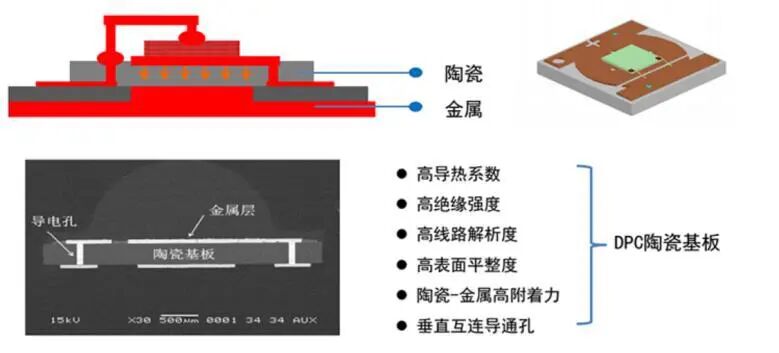
Schematic diagram of DPC ceramic substrate structure
1. Core Features of DPC Ceramic Substrates
High-Precision Circuit Fabrication Capability
The high-precision metal circuits formed on the surface meet the stringent requirements of flip-chip bonding, eutectic soldering, and other high-accuracy packaging techniques, supporting vertical interconnects and offering significant advantages in miniaturized, highly integrated electronic devices.
Excellent Thermal Conductivity
Commonly uses aluminum nitride (thermal conductivity: 170–200 W/(m·K)) or aluminum oxide (thermal conductivity: ~24 W/(m·K)) as the base material, delivering outstanding heat dissipation performance.
Good Coefficient of Thermal Expansion (CTE) Matching
By adjusting the ceramic material (e.g., AlN has a CTE of ~4.5 ppm/°C) and copper layer thickness, the substrate can be matched to the chip’s CTE, reducing thermal stress and enhancing device reliability.
Support for High-Reliability Packaging
Suitable for hermetic sealing and capable of withstanding harsh environments including high humidity, corrosion, and radiation, making it irreplaceable in critical fields such as automotive electronics.
DPC Ceramic Substrate Manufacturing Process
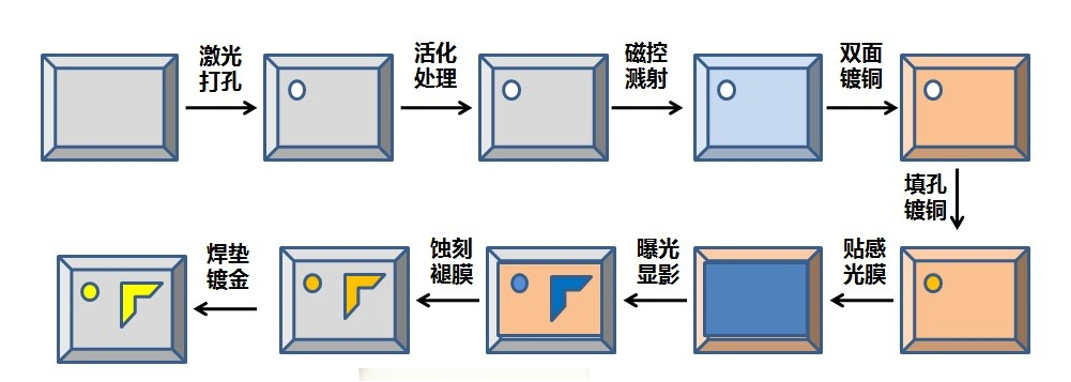
The core process flow can be summarized as: ceramic substrate → laser drilling → ultrasonic cleaning → PVD seed layer deposition and copper plating → exposure and development → resist stripping and etching.
3. Key Application Scenarios and Market Growth Outlook for 2026
DPC ceramic substrates are widely used in high-power LED lighting, automotive headlights, semiconductor lasers, power electronics, microwave communication, optical communication, VCSELs, and RF devices. Driven by the explosive growth of AI computing power and the advancement of automotive intelligence, AI servers and automotive LiDAR have emerged as key growth markets, significantly accelerating demand. Key application areas and projected growth data are summarized below:
Key Application Area | Projected Growth Data | Data Explanation |
|---|---|---|
Automotive Electronics – Intelligent Headlights | Market size reached RMB 293.5 billion in 2025 | Global automotive lighting market size, source: WENKH |
CAGR of 4.36% from 2023–2032, reaching RMB 395.7 billion by 2032 | Future market growth driven by automotive intelligence upgrades | |
Automotive Electronics – Automotive LiDAR | Penetration rate of factory-installed standard LiDAR exceeds 20% by 2026 | Significant growth in 2025 delivery volume and vehicle adoption; automotive segment is the primary demand driver |
AI Servers | Thermal conductivity is 300–600 times higher than traditional FR-4 material | Core technical advantage in solving thermal resistance issues in advanced HDI |
Embedding into HDI core reduces thermal resistance by over 70% | Enables efficient vertical heat conduction, ideal for high-power chip cooling | |
Optical Communication | InGaAs SWIR detectors typically have a height under 2mm | Compact packaging demands extremely high thermal management performance |
Wavelength stability maintained within ±1 GHz | Precision of Micro-TEC in independent temperature control for multi-channel optical modules |
1. Automotive Electronics: The “Thermal Management Core” for Intelligent Headlights and LiDAR
According to WENKH research, the global automotive lighting market reached RMB 293.5 billion in 2025, and is projected to grow at a CAGR of 4.36% through 2032, ultimately exceeding RMB 395.7 billion. The upgrade toward intelligent vehicles is the primary driver of this growth. As a critical component in high-power LED headlight thermal management systems, DPC ceramic substrates not only support chip mounting but also serve as the primary pathway for heat transfer to cooling systems, directly impacting headlight thermal efficiency and service life.
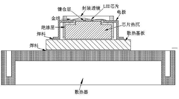
△ High-power LED device packaging structure (Source: FEA Works)
In the automotive LiDAR sector, both global shipment volumes and vehicle adoption rates surged in 2025, accelerating project implementation and commercialization. The automotive segment has become the dominant driver of LiDAR demand. It is expected that by 2026, the penetration rate of factory-installed standard LiDAR will exceed 20%, triggering a sharp increase in demand for high-performance ceramic substrates. Core components such as VCSELs and solid-state LiDAR operate at extremely high power densities, imposing stringent requirements on packaging substrates—including high-efficiency heat dissipation, thermal-electrical isolation, CTE matching, and compatibility with vacuum sealing. DPC ceramic substrates perfectly meet these demands with their high thermal conductivity, electrical insulation, fine-line precision, surface flatness, CTE matchability, and vertical interconnect capability.
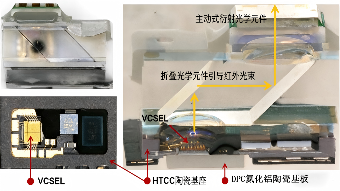
△ VCSEL disassembly image
2. AI Servers: The “Ultimate Solution” for Extreme Chip Cooling
The explosive growth of AI computing power places extreme demands on server thermal management. DPC ceramic substrates, with their exceptional thermal and mechanical properties, have become essential components in next-generation AI servers. Their integration into conventional PCBs represents a key technological approach to overcoming high-end server cooling challenges (substrates can use AlN or silicon nitride, with the latter enabling ultra-thin designs). Specific technical advantages include:
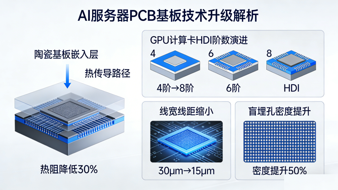
Solving Advanced HDI Thermal Resistance Challenges: Ceramic substrates offer 300–600 times higher thermal conductivity than traditional FR-4 materials. Embedding them into HDI cores can reduce thermal resistance by over 70%, enabling efficient vertical heat conduction and resolving cooling bottlenecks for high-power chips.
Addressing CowoP Packaging Stability Issues: Excellent CTE matching effectively disperses stress concentrations, preventing CowoP packaging failures and ensuring structural reliability in high-power, long-duration operating scenarios.
Meeting HBM Storage Cooling Demands: Rapidly dissipates heat conducted from TSVs (Through-Silicon Vias) to the substrate surface, preventing localized overheating that could cause TSV failure or increased read/write error rates—making it a critical thermal solution for large-scale HBM adoption.
3. Optical Communication: The “Critical Carrier Substrate” for Micro-TEC Coolers
With the rapid advancement of miniaturized optoelectronics, there is growing demand for compact, static, and long-life cooling solutions. Micro thermoelectric coolers (Micro-TECs) have emerged as a core thermal management solution for miniature electronic devices due to their high cooling power density, small size, low power consumption, and strong stability—making them a major research focus in thermoelectric cooling.
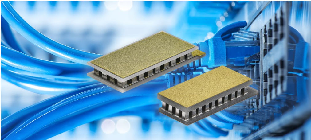
△ Micro-TEC for semiconductor laser cooling (Source: TTS)
Micro-TECs offer excellent thermal performance and integration advantages. Their carrier substrates must be high-quality ceramic or metallized boards to ensure strong solderability and, if needed, integrate thermistors. Key benefits include reliable mounting, low thermal resistance, efficient cooling, and high temperature control accuracy. Primary applications include:
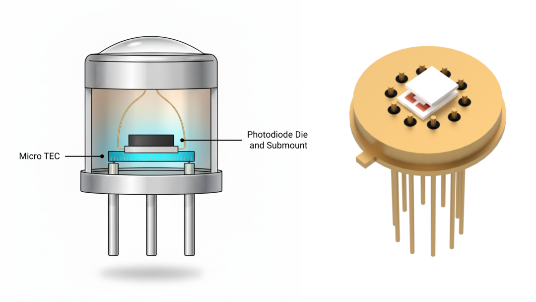
Photodetectors: For height-constrained devices like InGaAs short-wave infrared (SWIR) detectors (typically under 2mm) with limited heat dissipation paths, Micro-TECs enable precise thermal control when paired with control electronics, solving thermal management challenges in compact packages like TO-8 and stabilizing dark current and responsivity.
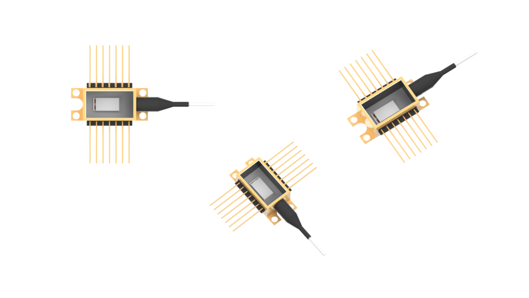
Optical Modules: In power-constrained data centers, Micro-TECs enable independent temperature control for each optical channel in multi-wavelength systems, achieving peak efficiency at moderate temperature differentials, maintaining wavelength stability within ±1 GHz, ensuring stable startup within seconds, and eliminating thermal crosstalk between adjacent channels.
Imaging Sensors: Imaging sensors used in spectroscopy, microscopy, machine vision, remote sensing, and medical diagnostics require extremely precise thermal management. Micro-TECs can be directly applied at the sensor location to provide solid-state cooling, ensuring stable low-light detection performance.
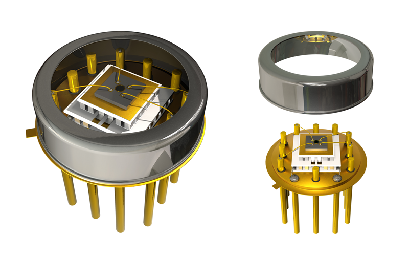
△ TO CAN packaged image sensor with MSX series thermoelectric cooler (Source: TTS)
4. DPC Ceramic Substrate Market Overview
According to QYResearch, the global DPC ceramic substrate market is projected to reach USD 252 million in sales by 2025. The high-brightness LED ceramic substrate market is highly concentrated, with the top seven global manufacturers accounting for approximately 70% of the market share.
By Application (2023 Data):
High-brightness LEDs account for approximately 56.6%, making it the largest application segment;
LiDAR & VCSEL represent about 24.9% and are expected to become the fastest-growing segment;
Thermoelectric coolers, high-temperature sensors, and RF/communication applications will also experience rapid growth.
From a downstream application perspective, high-brightness LEDs were the largest segment in 2023, accounting for 56.6% by value. The LiDAR and VCSEL segment held 24.9% and is projected to grow at the fastest pace—driven by the booming intelligent driving industry, where LiDAR, as a core hardware component, offers vast market potential and has become a key engine for China’s intelligent automotive transformation. Additionally, demand from thermoelectric coolers, high-temperature sensors, and RF/communication sectors will continue to rise rapidly, collectively driving the expansion of the global DPC ceramic substrate market. Amid ongoing technological evolution and rising market demands, BaiNeng YunBan has demonstrated strong competitiveness through its deep expertise in ceramic substrates: leveraging aerospace-grade precision manufacturing, its DPC substrates achieve 50-micron line/space resolution, meeting high-density packaging needs. Through precise selection and process optimization of high-quality AlN and Al₂O₃ materials, the company ensures stable high thermal conductivity and CTE matching, effectively addressing the stringent requirements of AI servers, automotive LiDAR, and optical communication Micro-TECs.
As a “Specialized, Sophisticated, Distinctive, and Innovative” enterprise, BaiNeng YunBan offers a diverse product portfolio including ceramic substrates, thick copper boards, and HDI boards, and provides customized solutions for high-end sectors such as automotive, medical, and defense electronics. With mature mass-production capabilities and consistent product quality, it plays a vital role in advancing the industrial adoption and application expansion of DPC ceramic substrates.
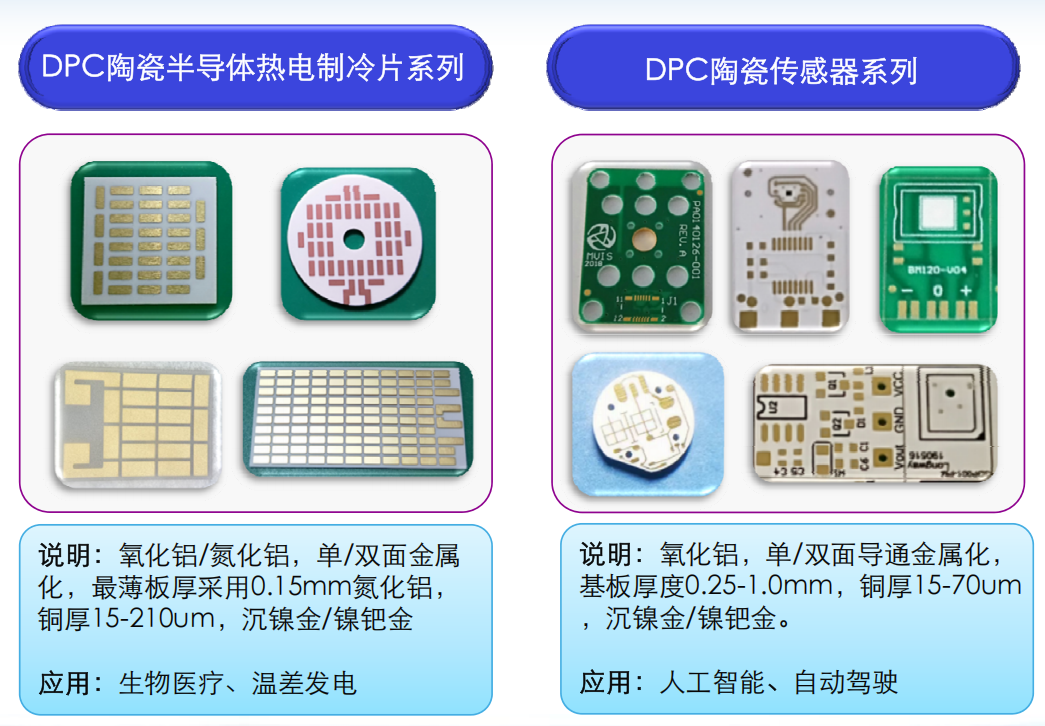
Selected DPC Ceramic Substrate Products from BaiNeng YunBan
trending news
Contact Us