



Sorry, no sales person is available right now to take your call. Pls leave a message and we will reply to you via email as soon as possible.
Home/ PCB News/ Comprehensive Analysis of the Advantages and Applications of PCB Embedded Technology
Comprehensive Analysis of the Advantages and Applications of PCB Embedded Technology
2026-02-03
Amid the trends of miniaturization in consumer electronics, high-frequency operation in communication devices, and high reliability in automotive electronics, traditional PCB surface-mount technology (SMT) is facing three major challenges: “insufficient space, signal attenuation, and reliability bottlenecks.” As smartphones, smart wearables, 5G base stations, and other products push integration density beyond physical limits, an innovative technology capable of “hiding” components inside the PCB—embedded PCB technology—is gradually becoming a core solution in high-end electronics manufacturing.
As a PCB manufacturer with years of industry experience, BAI NENG Yunban has consistently focused on advanced process R&D. Today, we’ll comprehensively unpack the core value, application scenarios, and key technical implementation points of embedded technology, exploring how it reshapes the design and manufacturing logic of electronic products.
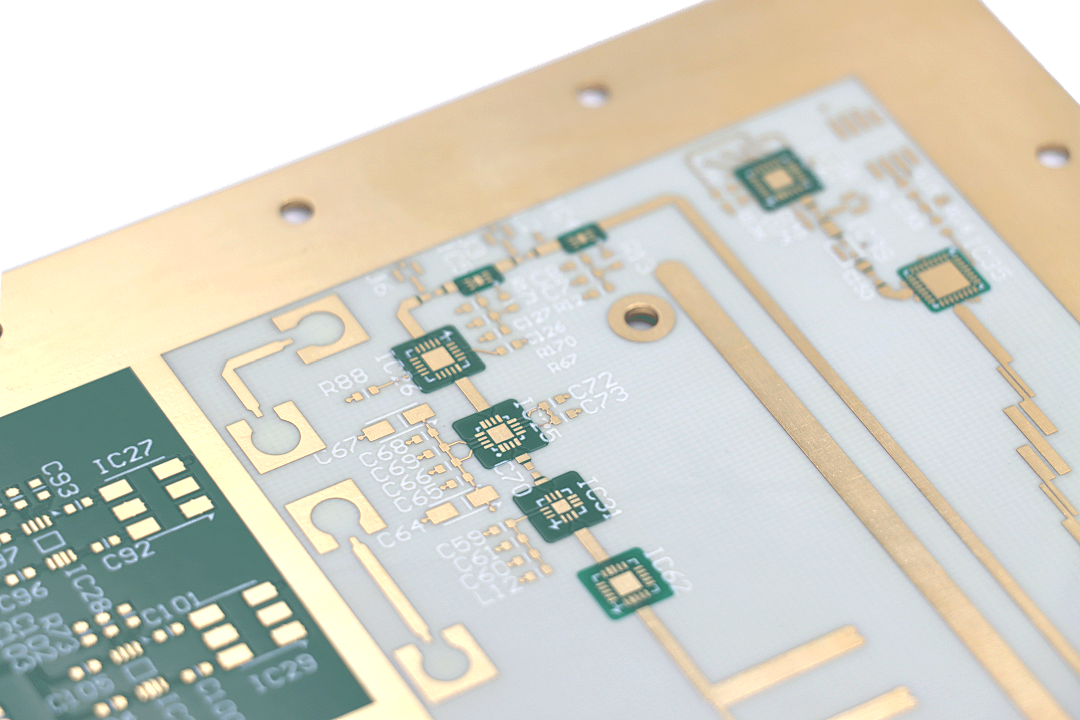
BAI NENG Yunban Embedded PCB Products
1. What Is Embedded PCB Technology? Breaking Free from the “Surface-Mount” Mindset
In simple terms, embedded PCB technology involves embedding passive components such as resistors, capacitors, and inductors—and even active components like diodes and miniature ICs—directly into the internal layers of the PCB substrate through processes like cavity milling, precise placement, and lamination, rather than mounting them on the board’s surface. Electrical connections between embedded components and external circuits are achieved via micro blind vias and buried vias within inner layers, creating an integrated structure of “components–substrate–circuitry.”
Compared to traditional methods, this “embedded” approach completely transcends the limitations of “surface real estate competition”—eliminating the need to reserve large surface areas for SMT components and avoiding performance losses caused by long leads—thus opening a new pathway for miniaturization and high-performance upgrades in electronic products.
2. Embedded vs. Traditional Processes: Five Core Advantages That Redefine Product Competitiveness
Overseas market research reveals that customers’ primary PCB requirements center on four dimensions: “smaller size, better performance, higher reliability, and lower total cost.” Embedded technology precisely addresses these needs, offering five key advantages:
1. Extreme Space Optimization Enables Product “Slimming”
Traditional PCBs often have their surface area heavily occupied by SMT components, limiting board size reduction or forcing compromises in functional integration. Embedded technology can free up 20%–30% of surface space, reducing overall PCB area by 15%–25%. For size-sensitive products like smartwatches, wireless earbuds, and implantable medical devices, this is nearly a “must-have” technology. For example, after embedding resistors and capacitors in a smartwatch’s main control board, more space becomes available for a larger battery or more complex sensor modules.
2. Enhanced High-Frequency/High-Speed Performance for the 5G/Millimeter-Wave Era
With the proliferation of 5G communications, automotive radar, and RF modules, signal integrity has become critical to product success. In traditional processes, long component leads introduce parasitic inductance and capacitance, causing high-frequency signal attenuation and severe crosstalk.
Embedded technology directly interconnects components with inner-layer circuits, shortening connection paths from millimeters to micrometers. This significantly reduces parasitic parameters, cuts signal delay by over 30%, and greatly improves electromagnetic interference (EMI) suppression. This is precisely why overseas manufacturers of 5G base stations and high-end RF modules are increasingly adopting embedded technology.
3. Doubled Reliability for Harsh Operating Environments
For customers in automotive electronics, industrial control, and aerospace, PCB reliability directly impacts product safety and service life. Surface-mounted components rely on solder joints for fixation and connectivity, which are prone to cracking or detachment under vibration, shock, and thermal cycling.
In embedded technology, components are fully encapsulated by the PCB resin substrate, acting as a “natural protective layer” that resists dust, moisture, and chemical corrosion while buffering mechanical stress. Solder joint count is reduced by over 40%, significantly lowering failure rates. BAI NENG Yunban’s test data shows that automotive ADAS module PCBs using embedded technology last more than twice as long as traditional ones in -40°C to 125°C thermal cycling tests.
4. Upgraded Thermal Management Solves Power Component Heat Dissipation Challenges
Heat dissipation for power components and highly integrated modules remains a persistent pain point in electronic design. In traditional processes, heat from surface components must travel through surface pads into the substrate via a single path, often creating hotspots. Embedded components, positioned closer to inner-layer substrates, benefit from shorter vertical heat paths. Combined with high-thermal-conductivity prepreg materials, inner-layer copper heat spreaders, and metallized thermal vias, they enable multi-dimensional heat dissipation channels for more uniform thermal diffusion and mitigation of localized overheating.
5. Simplified Assembly Balances Total Cost
Many customers worry about the high cost of embedded technology, but from a full-process perspective, it achieves cost balance by simplifying downstream assembly: fewer surface components mean shorter SMT and reflow processes, reduced consumption of fixtures and auxiliary materials, and lower transportation and warehousing costs due to smaller product size. For high-volume premium products, the total cost advantage of embedded technology becomes increasingly evident.
3. Which Applications Are Best Suited for Embedded Technology? Precise Alignment with Customer Needs
Embedded technology isn’t a “one-size-fits-all” solution, but its core value—miniaturization, high reliability, and superior performance—has been thoroughly validated across six major overseas application areas. Below, we present real-world cases with quantifiable results to illustrate how embedded technology solves critical customer pain points and empowers product innovation:
Consumer Electronics: Dual Breakthroughs in Ultra-Thin Design and High-Frequency Transmission—Core Challenge: Smart wearables and foldable phones demand extreme PCB thinness and size constraints while ensuring stable high-frequency signal transmission.
Case Study: A leading global smartwatch brand needed to integrate over 20 passive components and an RF module onto a 1.2mm-thick main control board. Traditional SMT failed due to insufficient surface space, forcing feature compromises. By adopting BAI NENG Yunban’s embedded technology to embed 15 passive components internally, 30% of surface space was freed, enabling PCB thickness reduction to 0.8mm. RF signal delay dropped by 25%, meeting Bluetooth 5.3 requirements, and battery capacity increased—boosting product battery life by 12%. Additionally, a top Chinese smartphone maker used embedded technology in the hinge-area PCB of its foldable phone, embedding microchips and inductors to solve component detachment issues during 200,000 folding cycles, improving reliability by 60%.
Communication Equipment: Ensuring Signal Integrity in 5G/Millimeter-Wave Applications—Core Challenge: 5G base stations and RF modules must overcome high-frequency signal loss and EMI while achieving high-density integration.
Case Study: A European 5G equipment vendor’s 77GHz automotive radar module suffered excessive insertion loss (>0.5 dB/inch at 10 GHz) due to long component leads in traditional PCBs, failing accuracy requirements. By embedding RF inductors and capacitors, connection paths were shortened from millimeters to micrometers, reducing parasitic inductance by 40%. Final insertion loss was controlled to below 0.18 dB/inch, achieving ±0.1° radar accuracy—fully meeting autonomous driving perception needs.
Automotive Electronics: Achieving High Reliability in Harsh Conditions—Core Challenge: ADAS systems and EV power modules must withstand thermal cycling and vibration; traditional SMT solder joints often fail.
Case Study: A global Tier 1 automotive supplier’s ADAS domain controller PCB had an 8% solder joint failure rate in -40°C to 125°C cycling tests using traditional SMT, failing ISO 26262 certification. After embedding core power devices and 12 resistors, solder joints decreased by 45%. Verified by BAI NENG Yunban, failure rate dropped below 0.5% after 500 thermal cycles, doubling service life. The solution is now mass-produced for Tesla, XPeng, and others. Another case: An EV inverter using chip-embedded PCB technology reduced stray inductance to below 1 nH and cut switching losses by 30%, perfectly supporting 800V platforms.
Industrial Control: Ensuring Long-Term Stability in Complex Environments—Core Challenge: Industrial robots and PLCs operate in dusty, vibrating, wide-temperature environments; PCB reliability directly affects downtime costs.
Case Study: A German industrial robot maker faced frequent resistor detachment in joint controllers due to high-frequency vibration, costing over €1 million annually in repairs. After embedding critical resistors and capacitors, components were fully resin-encapsulated, passing IP67 certification and running 10,000 hours at 2000 Hz vibration with zero failures—reducing maintenance costs by 90%.
Medical Devices: Balancing Miniaturization and Biocompatibility—Core Challenge: Portable diagnostics and implants require PCB miniaturization, biocompatibility, and high reliability.
Case Study: An overseas medical device company’s portable ultrasound probe needed PCB integration into a palm-sized head while meeting ISO 13485 biocompatibility standards. Embedded technology reduced PCB area by 25% and, combined with halogen-free substrate and OSP organic coating (withstanding 288°C/10s), fully met medical requirements—boosting probe battery life by 20%.
Aerospace: Dual Optimization for Lightweighting and Radiation Resistance—Core Challenge: Satellite comms and drones demand extreme PCB lightweighting, radiation resistance, and high integration.
Case Study: An overseas drone maker’s airborne comms module exceeded weight limits due to dense surface mounting, reducing flight time. By combining embedded technology with ceramic substrates to embed core circuits and passives, PCB weight dropped by 18%. It passed radiation testing (100 krad total dose) and improved signal stability by 35% in high-altitude low-pressure environments, meeting aerospace standards.
4. Implementing Embedded Technology: From Pain Points to Technical Solutions
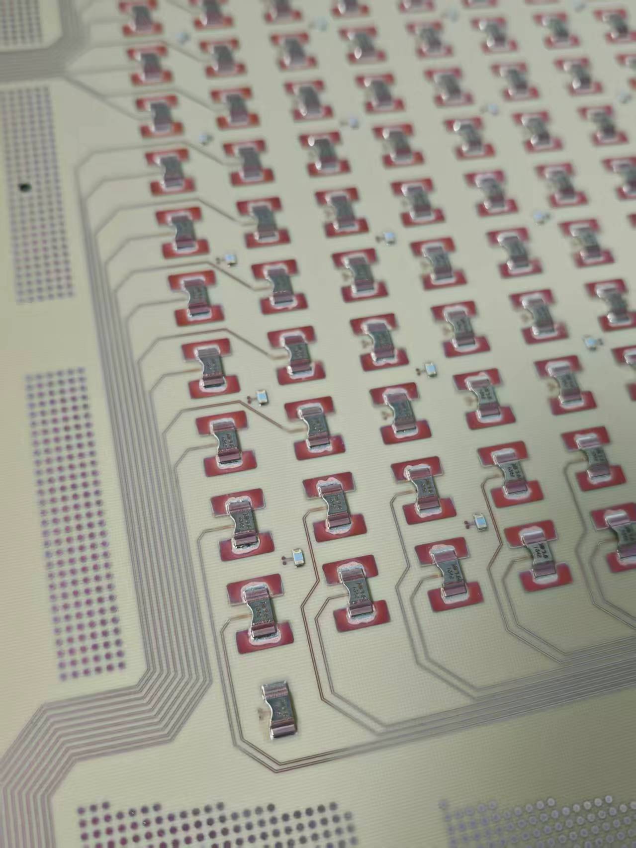
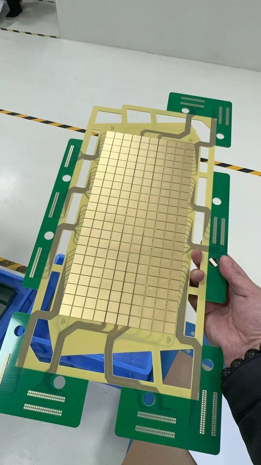
Successful implementation of embedded technology demands higher technical capabilities from PCB manufacturers, with key challenges in “component alignment accuracy, lamination control, interconnect reliability, and testing.” As a specialist in high-end PCB manufacturing, BAI NENG Yunban delivers stable embedded solutions through the following technical strengths:
High-Precision Alignment: Laser-marked fiducials combined with machine vision achieve ±5μm component placement accuracy, meeting micro-component embedding needs;
Optimized Lamination Process: Custom vacuum lamination profiles with staged temperature and pressure ramping prevent voids and uneven resin flow, ensuring tight component encapsulation;
Reliable Interconnects: Laser drilling plus plasma desmear precisely controls microvia depth, while electroless copper plating enhances adhesion for stable inner-layer connectivity;
End-to-End Testing: Multi-dimensional inspection including X-ray, AOI, and component value testing proactively mitigates batch risks.
5. Future Outlook: Embedded Technology Will Become Mainstream in High-End PCBs
As electronic product integration continues to rise, the conflict between “space” and “performance” will intensify. Embedded technology, as a core solution to this dilemma, is transitioning from niche high-end applications to mainstream adoption. In the future, combined with 3D embedding, heterogeneous integration, and AI-assisted design, it will enable even more complex component integration and superior performance—providing stronger support for overseas customers’ product innovation.
For PCB manufacturers, mastering embedded technology is not only a mark of technical prowess but also a key to capturing the high-end global market. BAI NENG Yunban remains customer-centric, continuously advancing R&D in advanced PCB processes to offer one-stop solutions—including embedded PCBs, ceramic substrates, HDI boards, and high-layer-count boards—helping global customers stand out in competitive markets.
Have you encountered space constraints or high-frequency performance degradation in your product designs? Feel free to share your challenges in the comments—we’ll provide professional process solutions!
trending news
Contact Us