



Sorry, no sales person is available right now to take your call. Pls leave a message and we will reply to you via email as soon as possible.
Home/ PCB News/ Baineng Yunban 10-layer Any-layer HDI PCB: Dedicated for high-end applications, featuring a high-performance any-layer interconnect solution
Baineng Yunban 10-layer Any-layer HDI PCB: Dedicated for high-end applications, featuring a high-performance any-layer interconnect solution
2026-06-12
With the rapid iteration and advancement of in-vehicle intelligence, industrial IoT, and embedded AI technologies, terminal electronic devices continue to evolve toward thinner, miniaturized designs, higher integration density, faster signal transmission, and enhanced operational reliability. Traditional multilayer PCBs, constrained by their manufacturing structure, can no longer meet the complex operating conditions and high-performance requirements of advanced devices. BaiNeng YunBan has long specialized in high-end HDI precision manufacturing and now proudly launches its 10-layer any-layer HDI PCB, leveraging leading-edge process capabilities and stable mass-production quality to precisely empower three core high-end sectors: in-vehicle intelligence, industrial IoT, and embedded AI—providing a robust foundational interconnect solution for premium electronic products.
I. Robust Precision Specifications: Building a High-Performance Hardware Foundation
BaiNeng YunBan’s 10-layer any-layer HDI PCB employs industry-leading any-layer interconnect technology combined with high-precision blind and buried via structures, completely overcoming traditional PCB routing limitations. Within an ultra-thin board profile, it achieves high-density layout and low-loss high-speed signal transmission while maintaining mechanical strength and long-term operational stability. All key process parameters fully align with high-end precision electronics standards, making it ideal for demanding applications.
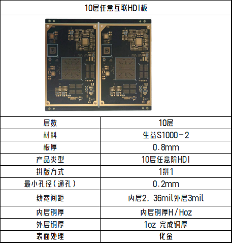
Process Highlights: The 0.8mm thin board paired with any-layer HDI architecture enables laser-drilled blind vias between any layers, complemented by inner-layer traces as fine as 2 mil and 0.2mm through-holes—significantly enhancing routing density and signal integrity. Shengyi S1000-2 material offers excellent thermal resistance and CAF (Conductive Anodic Filament) resistance, meeting the wide-temperature operational demands of automotive and industrial environments.
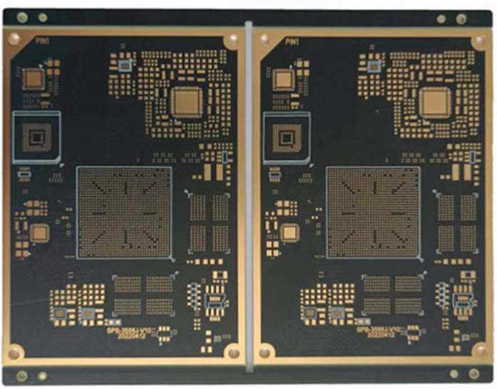
BaiNeng YunBan 10-Layer Any-Layer HDI Board
II. Scenario-Specific Adaptation: Stable Mass Production Across Three High-End Markets
Backed by stringent process standards and superior product performance, BaiNeng YunBan’s 10-layer any-layer HDI PCB has achieved scalable mass production, precisely tailored for three high-value domains: in-vehicle intelligence, industrial IoT & machine vision, and embedded AI education/research—addressing critical industry pain points with customized high-performance interconnect solutions.
01 In-Vehicle Intelligent Electronics | Automotive-Grade Reliability for Premium, High-Value Applications
Automotive electronics operate under harsh conditions—including rapid temperature shifts, constant vibration, and complex electromagnetic interference—demanding extreme stability, durability, and safety from PCBs. This 10-layer any-layer HDI PCB is ideally suited for core intelligent automotive hardware such as AI vision domain controllers, new energy vehicle gateways, high-definition dashcam computing motherboards, and in-vehicle infotainment hosts.
The any-layer interconnect architecture supports parallel transmission of multiple high-definition video streams and multi-protocol data, significantly reducing signal loss and latency;
High-Tg specialty substrate withstands an ultra-wide temperature range of -40℃ to 125℃, effectively preventing delamination and solder joint failure caused by thermal cycling;
High-quality ENIG (Electroless Nickel Immersion Gold) surface finish enhances soldering stability and oxidation resistance in complex automotive environments, extending equipment lifespan.
Implementation Case: Successfully deployed in infotainment systems and vision domain controllers for leading new energy vehicle manufacturers. Achieved 40% higher routing density and 25% lower signal transmission latency. Fully certified under AEC-Q100 automotive standards, with zero-failure delivery at a million-unit scale—validated by top-tier industry customers.
02 Industrial IoT & Machine Vision | Industrial-Grade Stability for High-Precision Computing Infrastructure
Designed for complex industrial environments featuring high humidity, dust accumulation, strong EMI, and extreme outdoor temperature variations, this product is fully compatible with industrial vision inspection motherboards, AI-enabled data acquisition gateways, PLC expansion modules, and photovoltaic energy storage monitoring terminals—delivering continuous, stable support for industrial intelligence.
10-layer independent stack-up design enables precise isolation of power, signal, and ground planes, greatly enhancing EMI immunity;
Low-CTE (Coefficient of Thermal Expansion) material minimizes thermal deformation during prolonged operation, ensuring ultra-high precision in machine vision inspection and data acquisition;
ENIG surface finish performs reliably in high-humidity, dusty outdoor conditions, eliminating solder oxidation and poor contact issues to ensure 24/7 stable operation.
Implementation Case: Mass-deployed in large-scale photovoltaic energy storage monitoring terminals. Achieved 99.98% operational stability under -20℃ to 85℃ conditions, with data acquisition error as low as 0.01%. Successfully passed State Grid-level reliability certification and is now widely implemented in major energy storage projects nationwide.
03 Embedded AI R&D & Educational Training | High Compatibility for Rapid Iteration and Innovation
Addressing the needs of embedded AI development—rapid iteration, multiple reflow cycles, and highly consistent batch performance—this product is optimized for NPU-based deep learning development boards, intelligent robot main control modules, and university AI innovation training platforms, fully supporting diverse scenarios including R&D testing, teaching labs, and prototype validation.
High-density any-layer interconnect structure supports multi-chip integration, accommodating high-end computing modules to meet complex AI workload scheduling demands;
Ultra-microvia precision工艺 accommodates fine-pitch computing chips, ensuring efficient and stable transmission of high-speed algorithms and massive data;
High-compatibility substrate withstands multiple reflow soldering cycles, ensuring exceptional batch-to-batch consistency and significantly reducing hardware failure rates and iteration costs in AI R&D and educational settings.
Implementation Case: Supplied core PCB hardware for AI training platforms at multiple universities, compatible with various mainstream NPU modules. Fully supports key training scenarios such as image recognition and edge AI inference. Motherboard repair rate is as low as 0.5%, reliably supporting daily teaching and algorithm prototype validation workflows.
III. End-to-End Dedicated Services: Full Lifecycle Support from R&D to Mass Production
Leveraging a mature and comprehensive high-end PCB R&D and manufacturing system, BaiNeng YunBan provides customers with a one-stop service covering technical enablement, rigorous quality control, and reliable delivery—ensuring efficient project execution at every stage:
Expert Technical Enablement: Experienced process engineers offer customized support including early-stage design review, impedance simulation, and routing optimization—proactively mitigating design flaws and mass-production risks to enhance overall product performance;
End-to-End Precision Quality Control: Fully automated smart manufacturing integrated with AOI optical inspection, X-ray non-destructive testing, and other multi-stage quality checks ensures precision and consistency across every production batch;
Highly Flexible Delivery Capability: Supports rapid small-batch prototyping and stable large-volume production, efficiently aligning with the R&D iteration and mass-production timelines of automotive, industrial, and AI innovation projects.
From the high-reliability demands of in-vehicle intelligence and the high-stability requirements of industrial IoT to the fast-iteration needs of embedded AI innovation, BaiNeng YunBan’s 10-layer any-layer HDI PCB precisely addresses three core challenges in advanced electronics: high-density layout, high-speed signal transmission, and high-reliability operation—thanks to its precision manufacturing, deep scenario adaptability, and proven mass-production stability. Moving forward, BaiNeng YunBan will continue to advance high-end HDI technological innovation, iteratively enhancing its products and service ecosystem to help customers improve quality, boost efficiency, reduce costs, and seize leadership in the high-end market.
trending news
Contact Us