



Sorry, no sales person is available right now to take your call. Pls leave a message and we will reply to you via email as soon as possible.
Home/ PCB News/ Comprehensive Introduction to PCB High-Frequency Boards and High-Frequency High-Speed Substrates
Comprehensive Introduction to PCB High-Frequency Boards and High-Frequency High-Speed Substrates
2026-06-11
1. Definition of High-Frequency PCBs
High-frequency PCBs are specialized printed circuit boards designed specifically for high-frequency and microwave applications, primarily suited for high-frequency scenarios operating at above 300 MHz (wavelength < 1 m) and microwave scenarios operating at above 3 GHz (wavelength < 0.1 m). The industry generally defines any printed circuit board with an operating frequency of ≥1 GHz as a high-frequency PCB.
These boards use microwave-specific copper-clad laminates as their core substrate material. They offer strong process compatibility—supporting both conventional rigid PCB manufacturing processes and customized precision processes tailored to product performance requirements. With the continuous evolution of electronic technologies such as 5G/6G communications, high-speed smart devices, microwave radar, and RF sensing, operating frequencies in electronic products are progressively shifting toward the 1 GHz microwave band and even the 30 GHz millimeter-wave band, driving increasingly stringent demands for high-frequency performance and stability in PCB substrates.
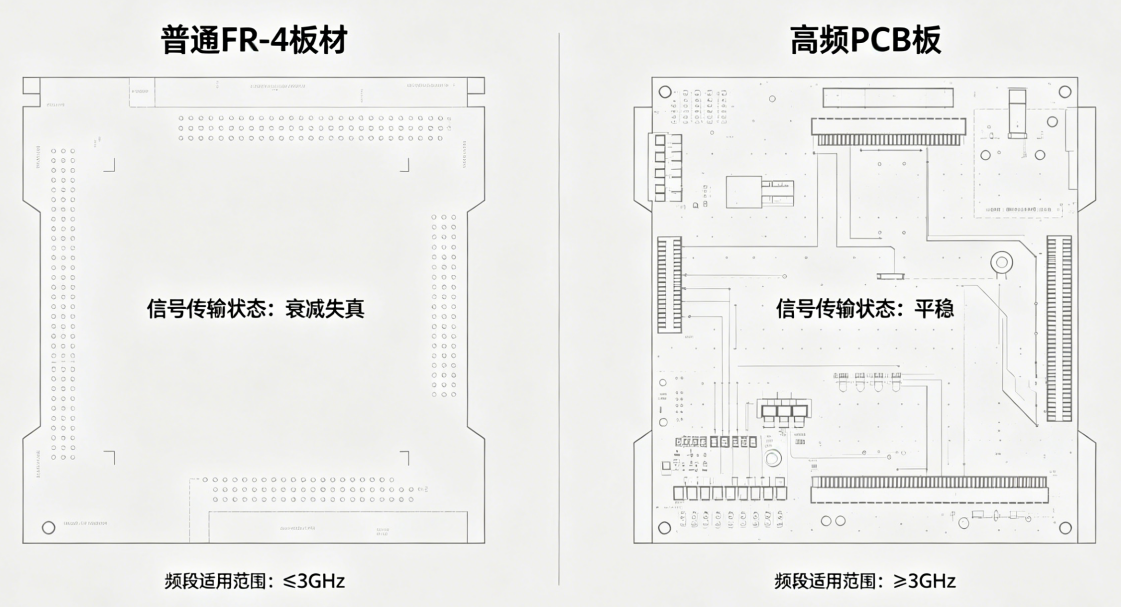
Compared to standard FR-4 materials, high-frequency substrates exhibit superior electrical characteristics and stable chemical properties, significantly reducing dielectric loss during high-frequency signal transmission and effectively mitigating issues like signal attenuation and waveform distortion caused by high-frequency effects. As such, they serve as essential foundational materials for high-frequency/microwave and high-speed transmission electronic devices.
2. Classification of High-Frequency PCB Materials and Core Manufacturing Processes
Currently, mainstream industrially mass-produced high-frequency PCB materials fall into two major categories. These substrates differ significantly in physical and electrical properties, requiring distinct production processes, process parameters, and posing unique processing challenges. Their specific characteristics and key process requirements are detailed below:
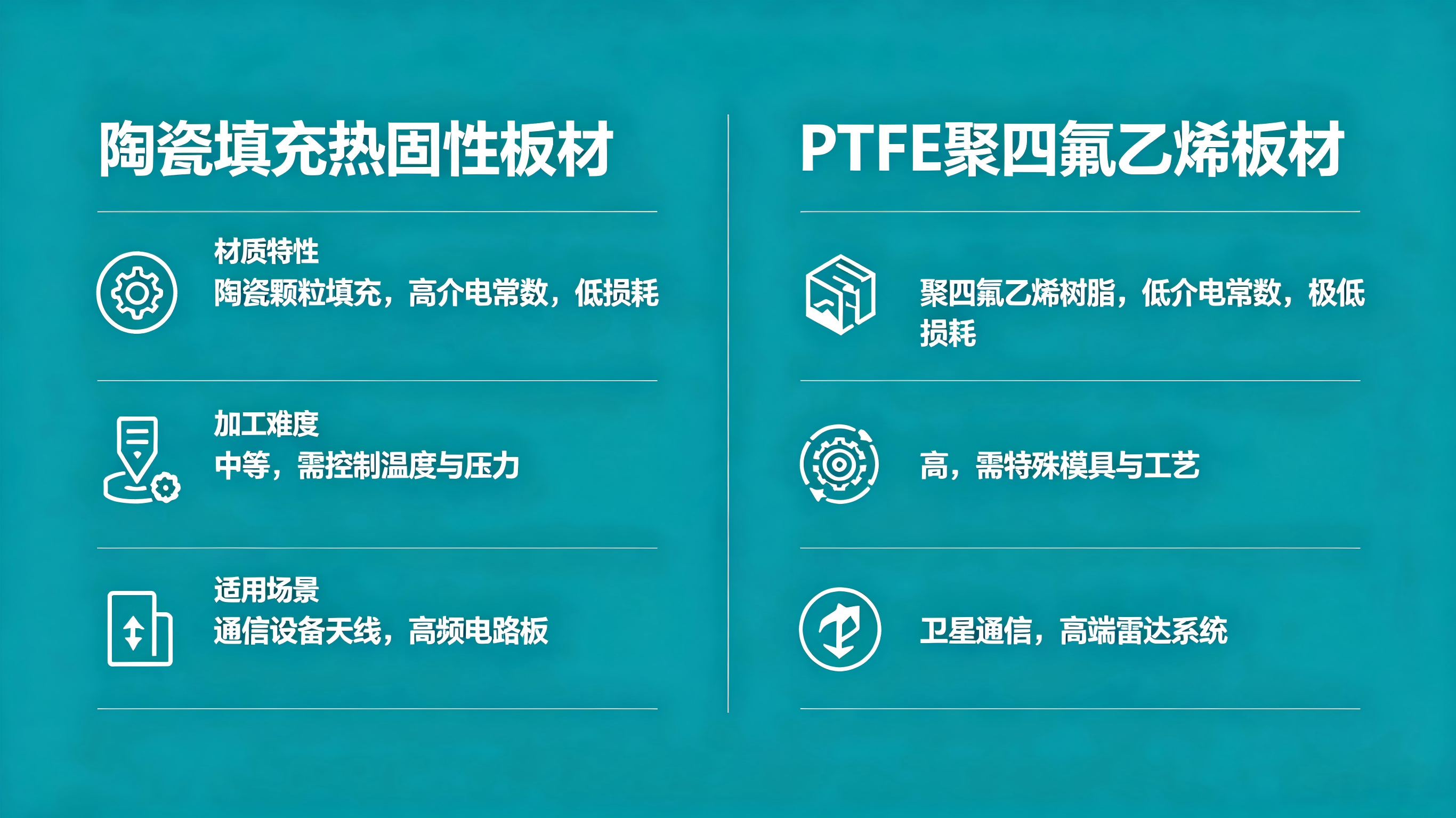
(1) Ceramic-Filled Thermoset High-Frequency Laminates
This type of laminate is a widely used mid-to-low-end high-frequency substrate. Its production process is highly compatible with conventional FR-4 epoxy-glass fabric laminates, allowing direct use of standard PCB manufacturing equipment. It offers excellent mass-production adaptability, mature processes, and controllable costs.
However, its main drawback lies in high brittleness and insufficient mechanical toughness, making it prone to chipping, board breakage, and substrate cracking during manufacturing. In precision machining operations such as drilling and routing, tool wear rates are significantly higher than with standard materials. Drill bits and routing tools typically have a service life about 20% shorter than when processing conventional FR-4. Therefore, strict tool wear management and regular tool replacement are critical during mass production to prevent processing defects.
(2) PTFE (Polytetrafluoroethylene) High-Frequency Laminates
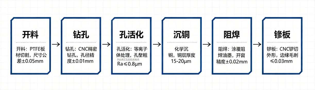
PTFE laminates are the core substrate material for high-end RF, microwave, and millimeter-wave applications. They offer extremely low signal transmission loss and excellent high-frequency electrical stability, making them the preferred choice for high-frequency, high-speed, and high-precision products. However, due to their inert surface and unique physical properties, PTFE materials are difficult to process and require a fully customized precision manufacturing process. Key process requirements for critical steps are as follows:
1. Material Cutting (Panel Preparation)
The original protective film on the material must remain intact throughout the cutting process. Direct contact between the panel surface and equipment tables or fixtures is strictly prohibited to prevent scratches, dents, oil stains, dust, and other surface defects, ensuring panel integrity.
2. Drilling
New standard #130 drill bits must be used exclusively, preferably in a single-panel-per-stack configuration. The drill press foot pressure must be consistently set to 40 psi. An aluminum entry sheet and a 1 mm melamine backup board should be used to securely clamp the panel, preventing movement and hole misalignment. After drilling, high-pressure air guns must thoroughly remove all dust residue from holes to avoid contamination affecting subsequent through-hole metallization. Additionally, high-stability drilling machines should be selected, strictly following the parameter control principle: “smaller hole diameter → higher drilling speed → lower chip load → slower retract speed.”
3. Hole Conditioning
Due to PTFE’s inert surface and poor adhesion, hole walls must undergo activation treatment to enhance the bonding strength of the subsequent electroless copper layer and ensure reliable via conductivity. Industry-standard methods include plasma activation and sodium-naphthalene etching, which effectively improve hole wall wettability and resolve issues like copper peeling and voids in plated holes.
4. PTH (Plated Through-Hole) / Electroless Copper Deposition
After micro-etching, the micro-etch depth must be strictly controlled to 20 micro-inches. Panels must enter the PTH line starting from the cleaning/degreasing tank. If initial metallization performance is unsatisfactory, rework is permitted—starting only from the pre-plate tank—to streamline the process and improve efficiency.
5. Solder Mask Application
Pre-treatment must use only acidic cleaning—mechanical brushing is strictly prohibited to avoid damaging the PTFE surface and degrading its electrical properties. After cleaning, panels must be baked at a constant 90°C for 30 minutes to completely remove moisture and contaminants before solder mask (green ink) printing and curing. Curing must follow a staged temperature profile: 30 minutes each at 80°C, 100°C, and 150°C, to ensure optimal solder mask adhesion and hardness. In case of solder mask peeling or delamination, the existing mask can be stripped, the surface re-activated, and the process repeated.
6. Routing (Profiling)
Before routing, white paper must be placed over the circuit side of the panel for protection. Double-sided fixtures should be used to clamp the panel securely. The clamping base material should be either 1.0 mm copper-free etched FR-4 or phenolic board, effectively buffering mechanical stress during machining to prevent panel cracking, surface abrasion, and circuit damage.
3. Core Electrical Properties of High-Frequency/High-Speed Materials (DK/DF Parameters)
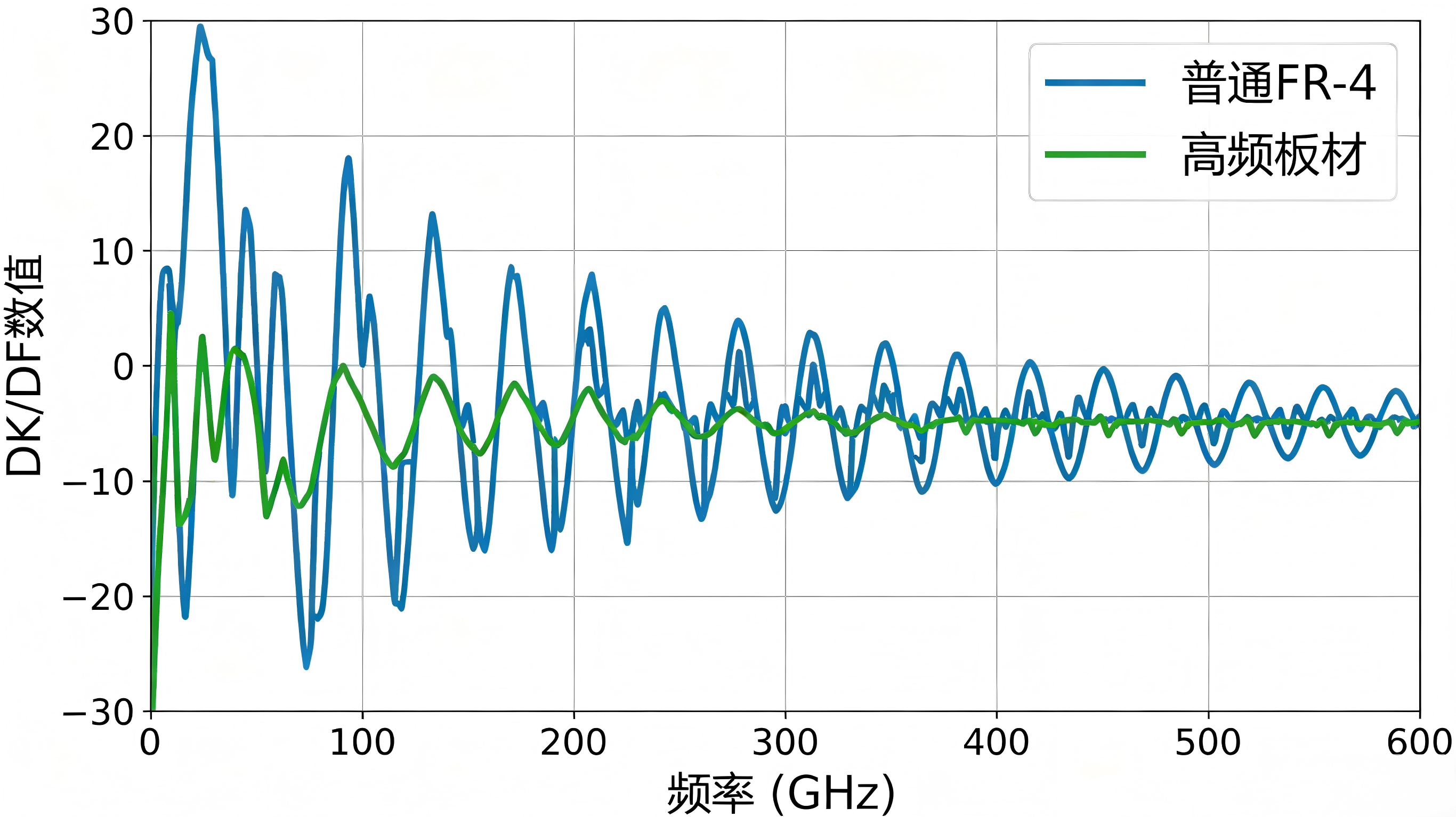
Dielectric constant (DK) and dissipation factor (DF) are the two most critical parameters for selecting high-frequency/high-speed PCB materials, directly determining signal transmission quality and circuit stability. DK governs the stability of signal transmission impedance and is fundamental to precise impedance control in high-frequency circuits. DF directly determines signal transmission loss and is key to achieving low-distortion, low-attenuation transmission of high-frequency and high-speed signals. Both parameters fluctuate with operating frequency and environmental temperature/humidity, and their stability varies greatly across different material types.
(1) Parameter Behavior of Standard Materials
Conventional FR-4 substrates exhibit high frequency sensitivity in DK and DF values, with the most significant fluctuations occurring between 1 MHz and 1 GHz. For example, a standard FR-4 material has a DK of 4.7 at 1 MHz, which drops to 4.19 at 1 GHz. Above 1 GHz, the change stabilizes, reaching approximately 4.15 at 10 GHz—showing an overall trend of slight decrease with increasing frequency.
Compared to DK, DF in standard materials is even more sensitive to frequency changes. Under high-frequency conditions, DF increases significantly with rising frequency, causing sharp rises in dielectric loss and worsening signal attenuation and distortion. This is the primary reason why standard FR-4 cannot support high-frequency or high-speed signal transmission.
(2) Parameter Behavior of High-Frequency/High-Speed Materials
Dedicated high-frequency/high-speed materials offer far superior parameter stability compared to standard FR-4, with strong resistance to frequency and environmental interference. Across the full 1 MHz–1 GHz range, high-quality high-frequency laminates can maintain DK fluctuations within ±0.02, showing only minimal attenuation with increasing frequency—delivering excellent impedance stability suitable for high-precision designs.
Regarding DF, premium high-frequency materials fall into two categories: one offers ultra-stable performance across all frequencies, with minimal DF variation under changing frequency or environmental conditions, ideal for complex multi-band applications; the other features ultra-low baseline DF values (though with variation magnitude similar to standard materials), fundamentally reducing high-frequency signal loss. Overall, the absolute value and stability of the DF parameter are the core criteria for evaluating a material’s high-frequency performance and classifying its grade.
4. Core Principles and Key Considerations for Selecting High-Frequency/High-Speed Materials
Material selection for high-frequency/high-speed applications requires balancing electrical performance, manufacturability, product reliability, and cost, matching the material precisely to the product’s frequency, data rate, and application scenario. Higher operating frequencies and faster signal speeds demand stricter requirements for low loss and high stability. In GHz-range high-speed circuits, standard FR-4 incurs excessive dielectric loss, easily causing signal integrity failure, waveform distortion, or transmission interruption—making it unsuitable for high-end applications.
Take a 10 Gb/s high-speed digital signal as an example: it is essentially a square wave composed of multiple sine wave harmonics, including a 5 GHz fundamental, 15 GHz third harmonic, 25 GHz fifth harmonic, and 35 GHz seventh harmonic—all falling within microwave bands. Such signals place extreme demands on edge steepness and transmission integrity. Consequently, material selection logic for high-speed digital circuits aligns closely with that for RF/microwave circuits, with core requirements being low dielectric loss, low signal distortion, and high parameter stability.
(1) Five Key Selection Criteria
1. Manufacturability and Reliability
Key checks include multilayer lamination compatibility, high-temperature thermal stability, CAF (Conductive Anodic Filament) resistance, mechanical toughness, and interlayer bonding reliability, along with verification of flammability rating compliance. Priority should be given to materials compatible with mass-production processes to avoid quality issues like delamination, substrate cracking, via failure, or layer misalignment—ensuring long-term product reliability.
2. Electrical Performance and Stability
Prioritize low-loss, stable DK/DF, and low dispersion coefficient materials to minimize parameter drift from frequency or environmental changes. Strictly control substrate thickness and resin content tolerances to ensure precise impedance control. For long high-speed traces, pair with low-roughness copper foil to further reduce skin-effect losses. Additionally, signal integrity simulation must be completed early in the design phase, with simulation results serving as the primary basis for material selection.
3. Material Supply Lead Time
Supply chains for custom high-end high-frequency materials often involve long lead times—typically 2–3 months for specialized grades—with limited inventory and extended delivery schedules. Only common grades like Rogers RO4350 are routinely stocked; niche or custom-parameter materials require advance production scheduling. Project teams must confirm material availability and lead times early in R&D to enable timely procurement and production planning, avoiding project delays due to material shortages.
4. Cost Appropriateness
Select materials based on product market positioning and application: for consumer-grade high-frequency products, prioritize cost-effective options that meet baseline performance; for high-reliability applications like telecom base stations, medical devices, industrial control, and aerospace/defense, prioritize performance and long-term stability, accepting higher costs.
5. Compliance Requirements
All selected materials must comply with global environmental regulations, meeting RoHS, halogen-free, and other relevant standards to satisfy certification and market access requirements worldwide, thereby mitigating compliance risks.
(2) Matching Data Rate with Material DF Value
Higher data rates demand stricter control of dielectric loss (lower DF values), requiring lower-loss substrates. Industry-standard DF ranges for common data rates are as follows:
DF 0.005–0.01: suitable for 10 Gb/s and below high-speed digital circuits;
DF 0.003–0.005: suitable for 25 Gb/s high-speed digital circuits;
DF ≤ 0.0015: suitable for 50 Gb/s and above ultra-high-speed digital circuits.
5. Leading High-Frequency/High-Speed Material Brands and Key Models
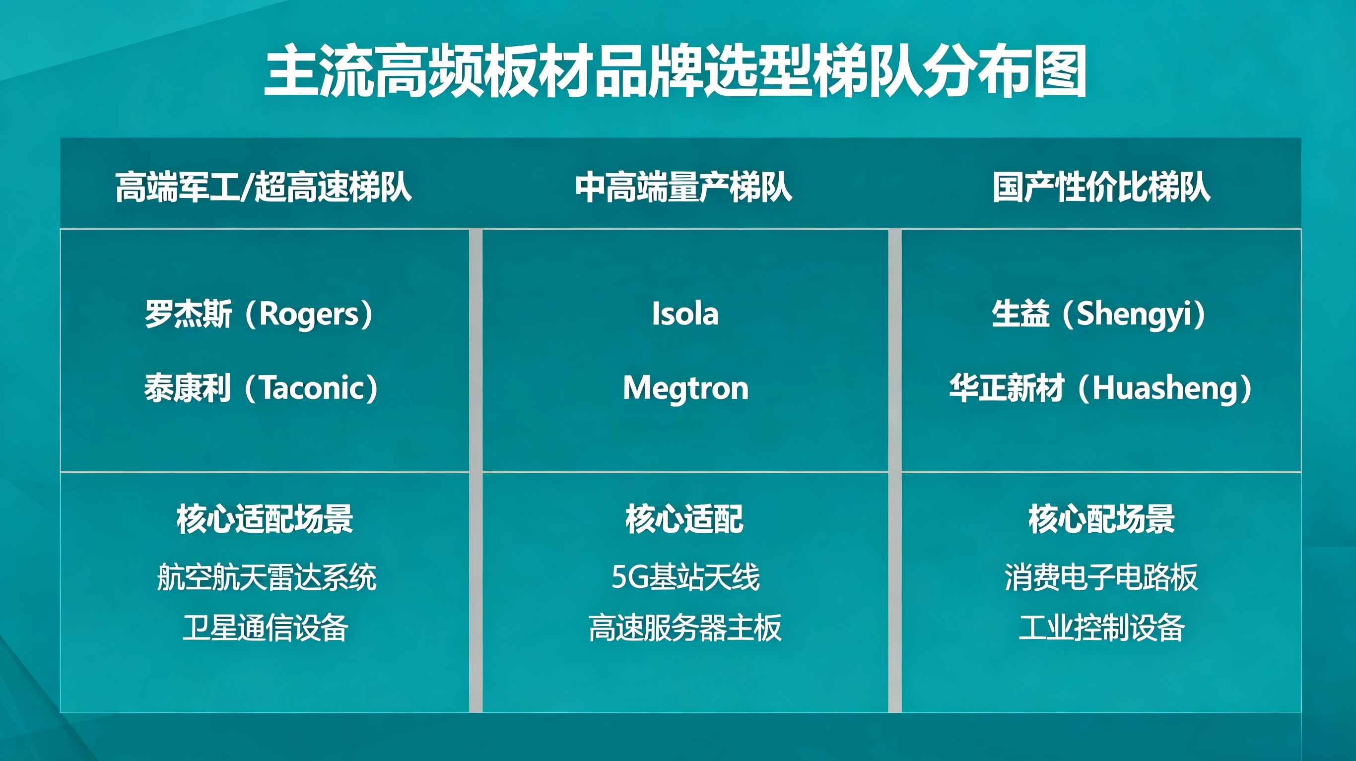
The global high-frequency/high-speed laminate market offers a comprehensive and well-structured product portfolio, with domestic and international brands covering all application scenarios—from consumer and industrial to telecom and defense. Key brands and representative models include:
1. Rogers Corporation (Premium RF Benchmark)
Global leader in premium high-frequency laminates, renowned for industry-leading electrical stability and ultra-low loss. Key models include RO4003, RO3003, RO4350, and RO5880, widely used in RF/microwave, millimeter-wave radar, 5G/6G infrastructure, and satellite communications.
2. TUC (Taiwan Union Technology) – High-Value Mid-to-High-End
Offers outstanding cost-performance ratio and excellent mass-production stability. Key models include Tuc862, 872SLK, 883, and 933, targeting mid-to-high-speed communication circuits and standard RF modules for volume manufacturing.
3. Panasonic – Leader in Ultra-Low-Loss High-Speed Digital
Specializes in ultra-low-loss high-speed laminates with exceptional parameter stability. Flagship Megtron4 and Megtron6 series are engineered for high-end servers, AI/ML computing hardware, and ultra-high-speed digital transmission.
4. Isola – Balanced Mass-Production Solution
Combines solid electrical performance with strong manufacturability. Core models FR408HR, IS620, and IS680 suit mid-to-high-end high-speed circuits and industrial RF equipment, ideal for scalable production.
5. Nelco – High-Stability High-Frequency Specialist
Known for excellent high-frequency parameter consistency and noise immunity. Key models N4000-13 and N4000-13EPSI are preferred for applications demanding stringent parameter stability.
6. Major Domestic Chinese Brands
Led by Shengyi (Dongguan), Wangling (Taizhou), and Taixing Microwave, these brands offer high cost-effectiveness and short lead times, fully meeting mass-production needs for mid-to-low-end high-frequency products and standard RF equipment, with strong advantages in domestic substitution.
7. Established International Suppliers
Includes Arlon (now part of Rogers) and Taconic (USA), both with decades of expertise in RF/microwave laminates. Their products deliver stable performance and ultra-low loss, enjoying high recognition in defense, aerospace, and premium microwave systems.
6. Comparison of Key Parameters, Advantages/Disadvantages, and Applications of Leading High-Frequency/High-Speed Materials
To address ambiguous engineering selection and mismatched application scenarios, the following table summarizes key electrical parameters, core strengths/weaknesses, production characteristics, and precise application matches for leading high-frequency/high-speed laminate brands and models—covering RF/microwave, high-speed digital, consumer mass production, and high-reliability defense applications.
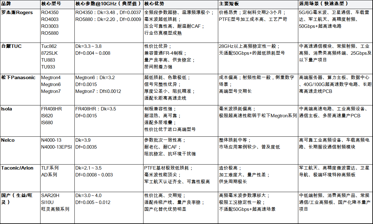
Key Takeaways for Brand Selection
1. Ultra-High Reliability + Millimeter-Wave RF: Choose Rogers, Taconic, or Arlon for defense, satellite, and advanced radar—prioritizing ultimate performance and stability over cost.
2. Ultra-High-Speed Digital Circuits: Opt for Panasonic Megtron or Isola’s premium series, optimized for signal integrity in data centers and high-performance computing.
3. Cost-Effective Mass Production: TUC series offers the best balance of performance, cost, and manufacturability—the optimal choice for consumer and industrial mid-to-high-end high-frequency volume production.
4. Domestic Cost Reduction & Supply Security: Shengyi, Wangling, and other Chinese brands are ideal for mid-to-low-frequency and standard high-frequency applications, significantly lowering project costs and supply chain risks.
trending news
Contact Us