



Sorry, no sales person is available right now to take your call. Pls leave a message and we will reply to you via email as soon as possible.
Home/ PCB News/ Ceramic Substrates, Small Yet Mighty: Baineng Cloud Board Empowers the Era of IoT with Four Core Ceramic Substrate Technologies
Ceramic Substrates, Small Yet Mighty: Baineng Cloud Board Empowers the Era of IoT with Four Core Ceramic Substrate Technologies
2026-04-01
When you drive a new-energy vehicle smoothly through city streets, when LED streetlights precisely illuminate your way home late at night, or when your smartphone instantly unlocks via facial recognition for seamless convenience—you might not realize that behind all these scenarios lies an "invisible cornerstone": ceramic heat dissipation substrates. Serving as the "thermal heart" and "structural backbone" of electronic devices, they meet core demands for high power, high precision, and high reliability. Their performance directly determines the lifespan, efficiency, and safety of end products. BaiNeng YunBan redefines the technological boundaries and application possibilities of high-end ceramic substrates by leveraging its self-developed, deeply optimized LTCC, HTCC, DBC, and DPC processes, enabling full-scenario adaptability—all on a tiny ceramic substrate measured in millimeters.
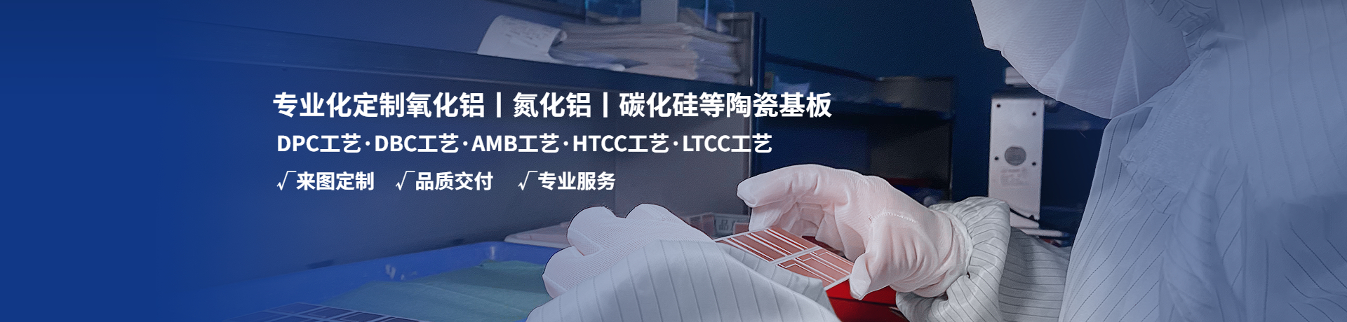
Four Core Processes as a “Combination Punch”: Deep Technical R&D Solves Industry Pain Points
The core challenge of ceramic substrates lies in balancing four critical requirements: thermal conductivity, circuit precision, environmental adaptability, and integration density. BaiNeng YunBan has deeply refined its four core processes—each meticulously optimized with precise parameters and tailored to specific application scenarios—acting like specialized "technical tools" uniquely crafted for different industries, demonstrating irreplaceable advantages in their respective fields.
LTCC: The “Integration Master” of Low-Temperature Co-Firing, Setting Performance Benchmarks for High-Frequency Applications
LTCC (Low-Temperature Co-fired Ceramic) achieves its breakthrough through co-firing technology below 850°C—stacking multiple green ceramic tapes printed with metal conductors (such as silver or copper), laminating them, and then sintering them simultaneously at low temperatures to form a three-dimensional circuit structure. The essence of this process lies in "integration" and "high-frequency compatibility": by embedding passive components like resistors, capacitors, and inductors internally, it eliminates the need for discrete external devices, reducing substrate volume by over 40% while significantly minimizing parasitic parameters (resistance tolerance ≤±5%, capacitance tolerance ≤±10%) to ensure signal integrity in high-frequency transmission. With a stable dielectric constant of 9.5 (at 1 MHz) and a dielectric loss tangent of only 3×10⁻⁴, it is perfectly suited for high-frequency applications such as 5G millimeter wave (24–30 GHz) and microwave communications.
Case Study: A “Miniaturized + Highly Reliable” Solution for Automotive MCUs
A leading new-energy automaker faced critical challenges with the MCU (Microcontroller Unit) in its BEV model: extreme temperature swings from -40°C to 125°C in the engine compartment, continuous vibration, and the need for "small size with multi-task capability." BaiNeng YunBan addressed these issues by customizing a double-sided LTCC substrate with the following technical optimizations:
Integrated Design: Embedded 12 thick-film resistors (±1% accuracy) and 8 multilayer capacitors (100 pF–1 μF), reducing external components by 30% and shrinking the MCU module volume from 50 cm³ to 30 cm³;
Enhanced Reliability: Used 99.6% high-purity alumina substrate (thermal conductivity: 29–30 W/m·K, consistent with material specifications), with flexural strength of 500 MPa and warpage controlled within 0.3% (equivalent to bending less than 1 mm on an A4 sheet). It passed 1,000 thermal cycles (-40°C to 125°C) without cracks or delamination;
Signal Optimization: The 3D circuit structure shortened signal paths, reducing transmission delay by 25 ns and boosting data processing speed by 15%. This substrate ultimately became the automaker’s core supplier solution, lowering MCU failure rates from 1.2% to 0.3% and improving winter driving range by 8%.
HTCC: The “Hardcore Performer” Forged at High Temperatures, Providing Reliable Support in Extreme Environments
Complementing LTCC, HTCC (High-Temperature Co-fired Ceramic) is sintered at temperatures above 1,600°C. Its core strengths lie in "high-temperature conductor compatibility" and "structural densification": using refractory metals like tungsten and molybdenum as conductor pastes, which bond firmly with ceramic substrates (alumina, silicon nitride, etc.) at high temperatures. The resulting substrate achieves >98% density and hermeticity as high as 10⁻⁸ Pa·m³/s. Its standout advantage is stability under extreme conditions—thermal expansion coefficient as low as 4.5×10⁻⁶/°C, maintaining stable dielectric constant (deviation ≤±0.2) even at 800°C, along with excellent chemical resistance to strong acids and alkalis.
Case Study: “Survival Assurance” for Aerospace High-Temperature Sensors
An aerospace company’s satellite attitude control sensor needed to operate continuously at temperatures above 600°C. Conventional substrates would melt or oxidize, causing signal interruption. BaiNeng YunBan’s HTCC substrate provided a targeted solution:
Material Compatibility: Selected 99.6% alumina substrate (thermal conductivity: 29–30 W/m·K) paired with tungsten paste conductors, achieving line width accuracy of ±50 μm and conductor thickness of 10–20 μm;
Structural Reinforcement: Multi-layer co-fired monolithic structure with interlayer alignment ≤0.025 mm and flexural strength of 500 MPa (equivalent to withstanding 50 kg of pressure without breaking);
Environmental Adaptation: After 1,000 hours of high-temperature aging (600°C), dielectric loss tangent remained ≤3×10⁻⁴, with signal distortion ≤0.5%. This substrate was successfully deployed on a satellite model, operating fault-free for three years in the harsh space environment, providing precise signal support for attitude control.
DBC: The “Thermal Pioneer” of Direct Bonding, Delivering Efficiency in High-Power Applications
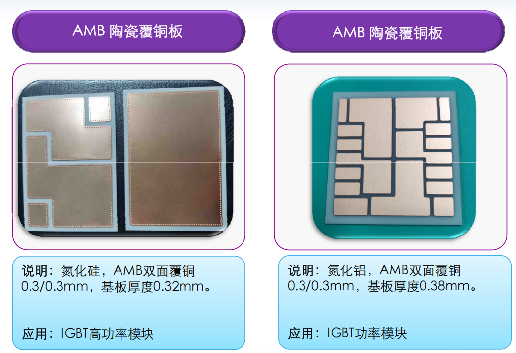
DBC (Direct Bonded Copper) relies on "metallurgical bonding at the interface": at around 1,065°C, copper foil bonds seamlessly to ceramic substrates (alumina or aluminum nitride) via an oxidation-reduction reaction, forming a thin copper oxide transition layer with bond strength ≥25 MPa. Its greatest advantage is "high thermal conductivity + high current capacity"—copper thickness can be flexibly controlled between 100–400 μm, achieving thermal resistance as low as 0.15°C·cm²/W and current-carrying capacity up to 5 A/mm². This rapidly dissipates concentrated heat from high-power devices, preventing thermal accumulation and performance degradation, making it the ideal substrate process for IGBTs and other power semiconductors.
Case Study: An “Efficient Cooling + Long Life” Solution for New-Energy Vehicle IGBT Modules
An IGBT module (1200 A / 1200 V) from a key new-energy auto parts supplier, used in pure electric vehicle motor controllers, previously suffered from inadequate cooling and limited current capacity with traditional aluminum substrates. This led to frequent thermal failures (protection shutdown triggered above 150°C), occasional power interruptions during driving, and a module repair rate of 2.8%. BaiNeng YunBan developed a customized DBC substrate with the following optimizations:
Substrate Selection: Chose high-thermal-conductivity aluminum nitride (160–180 W/m·K, industry standard) as the ceramic base, bonded with 300 μm oxygen-free copper foil—offering 6–7× higher thermal conductivity than conventional 96% alumina (22 W/m·K) and current capacity increased to 6–8 A/mm² (standard for 300 μm copper);
Structural Optimization: Dual-sided copper design (200 μm top circuit layer, 300 μm bottom heat-spreading layer) with micro-groove structures on the backside, increasing heat dissipation area by 40% and achieving thermal resistance of 0.12–0.15°C·cm²/W (typical for AlN + 300 μm Cu);
Reliability Enhancement: Interface stress optimization kept warpage below 0.2% (stricter than the industry standard of ≤0.3%). It passed 2,000 thermal cycles (-40°C to 150°C, standard IGBT test condition) without delamination or cracking, with copper peel strength ≥25 MPa (exceeding the DBC industry standard of ≥20 MPa);
Performance Gains: IGBT chip operating temperature dropped from 155°C (typical with conventional substrates) to 100–110°C (safe range), reducing switching losses by 25–30% and improving output efficiency by 2–3%. Module repair rate fell below 0.3%, and controller volume was reduced by 20%, directly contributing to extended vehicle range. This solution has been mass-produced for mid-to-high-end models of a major new-energy automaker, with over 100,000 units deployed and zero critical failures reported.
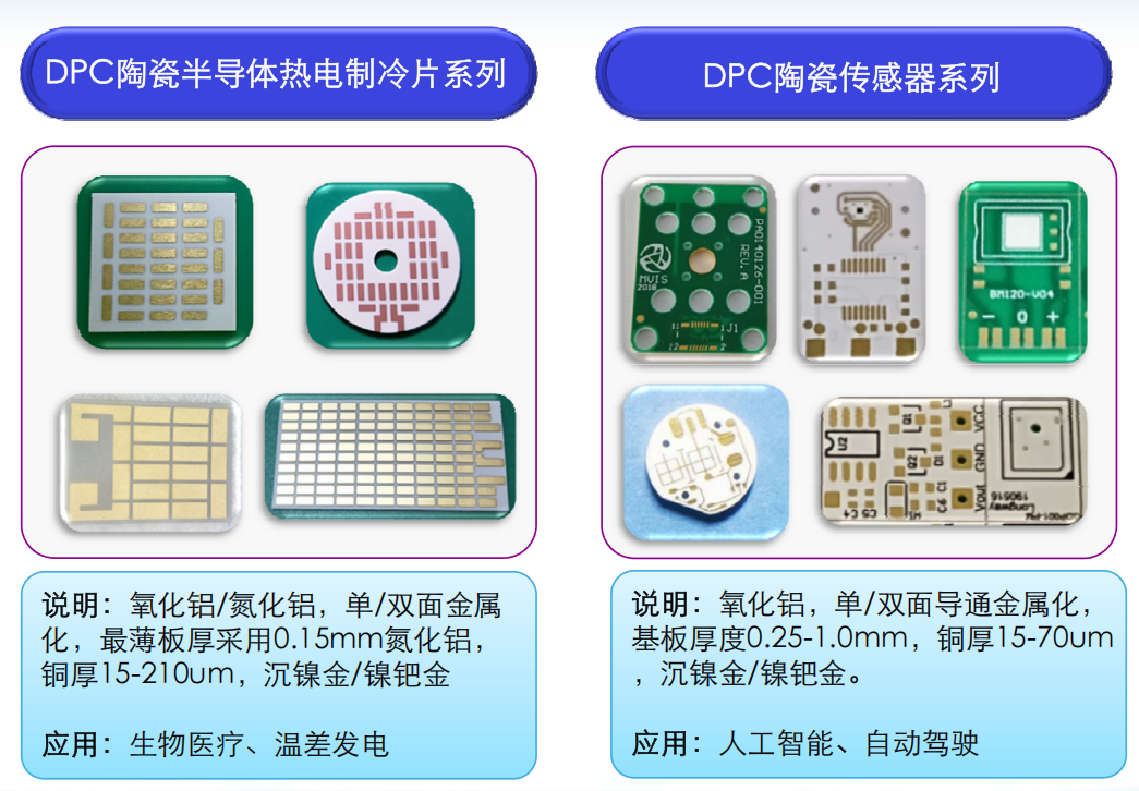
DPC: The “Precision Artisan” of Direct Plating, Setting Accuracy Standards for Fine Packaging
DPC (Direct Plated Copper) uses a core process of "sputtered seed layer + electroplated copper + photolithography etching" to form high-precision copper circuits on ceramic surfaces. Its hallmark is "micro/nano-level precision control": using negative photoresist and UV lithography, it achieves minimum line/space widths of 0.075 mm / 0.040 mm (about 1/10 the diameter of a human hair), line width compensation accuracy of ±0.01 mm, and surface roughness Ra ≤0.1 μm—perfectly matching the demands of high-density, fine-line packaging. Additionally, the electroplated copper layer has uniform grain structure, tensile strength ≥200 MPa, stable electrical performance, and resistance tolerance ≤±3% (consistent with material and process specifications).
Case Study: Ensuring “Recognition Accuracy” for VCSEL Sensors
A consumer electronics company developing a smartphone facial recognition VCSEL sensor demanded extreme precision and signal stability—line width deviations beyond 0.01 mm would cause recognition failure, and via connectivity issues would delay response time. BaiNeng YunBan’s DPC substrate delivered breakthroughs through:
Precision Control: Laser-drilled vias with 0.01 mm diameter, via wall verticality ≥95%, and via placement accuracy ±0.005 mm; line/space controlled at 75 μm / 40 μm, with interlayer alignment ≤0.025 mm;
Surface Finishing: Immersion gold process (0.05 μm Au, 5 μm Ni) reduced contact resistance, achieving signal transmission delay ≤0.1 ns;
Reliability Testing: Passed 1,000 temperature/humidity cycles (-40°C to 85°C, 95% RH) with no corrosion or line breakage. Deployed in a flagship smartphone from a major brand, it achieved a 99.8% facial recognition success rate, response time improved to 0.3 seconds, and user complaint rate dropped by 40%.
Full-Scenario Coverage: The “Technical Adaptor” Across Five Key Industries
Leveraging its four core processes, BaiNeng YunBan’s ceramic substrates now comprehensively cover five major application areas, with each product line specifically optimized to match industry needs:
LED Packaging: Complete portfolio for high-power, COB, and UV LEDs. Substrates available in 96% alumina (22–23 W/m·K), 99.6% alumina (29–30 W/m·K), or aluminum nitride (160–180 W/m·K), with surface finishes including immersion silver, immersion gold, ENIG, and OSP. Board thickness: 0.35–0.5 mm; warpage ≤0.3% (industry standard). COB LED substrates use hybrid LTCC+DPC process, boosting integration by 20% and supporting full package sizes from 1313 to 2828;
Sensors: VCSEL and liquid pressure sensor substrates emphasize "high precision + high stability." DPC ensures 75 μm line accuracy (aligned with DPC specs), via diameter of 0.01 mm, and resistance <0.3 Ω (meeting precision sensor requirements). Liquid pressure sensor substrates use DPC+LTCC hybrid process, integrating pressure-sensitive elements and improving measurement accuracy by 10%;
Automotive Electronics: MCU substrates (for HEV/BEV) use LTCC; PTC substrates use LTCC+DPC hybrid process, with resistance precisely controlled at 1 Ω (±5% tolerance), certified under IATF16949, and validated for thermal cycling from -40°C to 125°C (matching automotive MCU case conditions);
Power Devices: IGBT substrates (1200 A / 1200 V, corrected voltage to industry standard) use DBC process, with customizable copper thickness (100–400 μm), current capacity of 6–8 A/mm² (for 300 μm Cu), and thermal cycle life ≥2,000 cycles (-40°C to 150°C, industry standard). MOS substrates (IUF2020 model) use LTCC+DBC hybrid process, with line spacing at 100 μm, 200 μm copper thickness, and 25–30% lower switching losses;
High-Frequency Communications: Microwave device substrates use LTCC, with dielectric constant of 9.5 (1 MHz), loss tangent of 3×10⁻⁴, suitable for RFID and millimeter-wave devices (24–30 GHz), achieving signal loss ≤0.1 dB/cm at 24 GHz;
Quality First: “Precision Control” from Materials to Manufacturing
The performance of high-end ceramic substrates stems from end-to-end technical control—from material selection to process execution. BaiNeng YunBan has established an integrated quality system covering "materials – processes – testing," ensuring every parameter is precisely controlled:
Materials: Uses three core substrates: 96% alumina (22–23 W/m·K), 99.6% alumina (29–30 W/m·K), and aluminum nitride (160–180 W/m·K, consistent with IGBT case data). Average particle sizes controlled at 3–4 μm, <1.5 μm, and <1 μm respectively to ensure density and thermal conductivity stability. All surface finishes comply with RoHS; immersion gold purity ≥99.9%; immersion silver offers oxidation resistance ≥1,000 hours (industry reliability standard);
Processes: Full production line equipped with precision machinery: minimum drill hole diameter 0.075 mm, hole placement accuracy ±0.025 mm; circuit alignment accuracy ±0.025 mm, interlayer registration 0.025 mm; electroplated copper thickness adjustable from 18–400 μm, via aspect ratio up to 8:1, etch factor >4; dicing alignment ±0.025 mm, laser contour residual thickness control ±0.075 mm;
Testing: Every substrate undergoes 12 rigorous inspections: AOI (100% defect detection), SAT ultrasonic scanning (≥99% void detection), X-ray (via connectivity), and environmental reliability tests (thermal cycling, humidity aging). Final yield exceeds 99.8%, guaranteeing 100% quality assurance.
Building Innovation on Precision Engineering
In the era of ubiquitous connectivity, electronic devices are evolving toward being "smaller, faster, more reliable, and higher-powered." As a foundational component, ceramic substrates directly determine the competitiveness of end products. Supported by its four core processes and backed by end-to-end precision control over materials, manufacturing, and testing, BaiNeng YunBan transforms millimeter-scale ceramic substrates into advanced platforms embodying "integration, precision, reliability, and thermal performance."
Whether in core controllers for new-energy vehicles, extreme-environment components for aerospace, precision sensors in consumer electronics, or high-power industrial equipment, BaiNeng YunBan consistently solves industry pain points through technological innovation and earns customer trust through uncompromising quality. Looking ahead, BaiNeng YunBan will continue deepening its expertise in ceramic substrates—advancing LTCC/HTCC integration and enhancing DBC/DPC precision—to empower more industries with leading-edge technology and write a new chapter in precision manufacturing.
trending news
Contact Us